Light emitting device

a technology of light emitting device and light source, which is applied in the direction of semiconductor devices, lighting and heating apparatus, semiconductor devices for light sources, etc., can solve the problems of reducing the luminous flux of the light emitting device and the inability to achieve the desired long life, etc., and achieves the effect of improving sulfurization resistance and high lumen maintenan

Active Publication Date: 2020-04-02
NICHIA CORP
View PDF2 Cites 0 Cited by
  • Summary
  • Abstract
  • Description
  • Claims
  • Application Information

AI Technical Summary

Benefits of technology

[0014]According to one embodiment of the present disclosure, a light emitting device that is improved in sulfurization resistance and has a high lumen maintenance can be provided.

Problems solved by technology

However, the sealing member made of a composite containing an epoxy resin tends to discolor to yellow due to light and heat emitted from the light emitting element with an increased output power, which may cause change in the color of the light emitted from the light emitting device, so that the desired long lifetime may not be achieved.
Furthermore, the sealing member a composite containing a silicone resin has high gas permeability and tends to transmit air, so that the silver plating used in the light emitting device discolors over time due to sulfides in air, which may result in reduction of the luminous flux of the light emitting device.

Method used


Image

  • Light emitting device
  • Light emitting device
  • Light emitting device

Examples


example 1

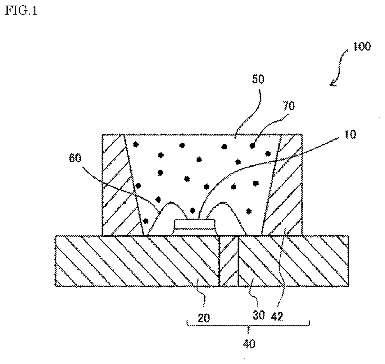
[0094]The package member 42 having the recess constituting the side wall and the substrate 40 having the plurality of conductive members 20 and 30 constituting the bottom portion of the recess of the package member as shown in FIG. 1 were prepared. A nitride semiconductor having a light emission peak wavelength of 450 nm as the light emitting element 10 was mounted on the one conductive member 20, and the light emitting element 10 was electrically connected to the conductive members 20 and 30 respectively with the wires 60.

[0095]The silicone composite used was a thermosetting dimethylsilicone resin containing the component (A), the component (B), and the component (C) (OE6351, a trade name, produced by Dow Corning Toray Co., Ltd.). The content of the component (C) was as small as 500 ppm (0.05% by mass) or less in the thermosetting dimethylsilicone resin, and thus the amount of the thermosetting dimethylsilicone resin was assumed to be the total amount of the component (A) and the c...

example 2

[0096]A light emitting device was produced in the same manner as in Example 1 except that a silicone composite containing 0.3 part by mass of the zinc silanolate as the component (D) was added to 100 parts by mass of the thermosetting dimethylsilicone resin.


PUM

PropertyMeasurementUnit
peak wavelengthaaaaaaaaaa
peak emission wavelengthaaaaaaaaaa
peak wavelengthaaaaaaaaaa

Abstract

A light emitting device includes a light emitting element, a substrate which contains a conductive member containing silver having the light emitting element mounted, and a sealing member which covers the light emitting element, and the sealing member is made of a cured silicone composite containing the following components (A), (B), (C), and (D):
    • (A) an organopolysiloxane containing at least two alkenyl groups each bonded to a silicon atom per one molecule;
    • (B) an organohydrogenpolysiloxane containing at least two hydrogen atoms each bonded to a silicon atom per one molecule;
    • (C) a hydrosilylation catalyst; and
    • (D) a zinc silanolate represented by the following formula (1):
In the formula (1), R1 to R7 each independently represent a linear, branched, or cyclic monovalent hydrocarbon group having 1 to 10 carbon atoms, which may be substituted by a fluorine atom, or each independently represent a hydroxy group or an alkoxy group; and m represents an integer of 1 or greater.

Description

CROSS-REFERENCE TO RELATED PATENT APPLICATION[0001]This application claims priority to Japanese Patent material No. 2018-184045, filed on Sep. 28, 2018, and Japanese Patent Application No. 2019-166348, filed on Sep. 12, 2019, the entire disclosures of which are incorporated herein by references in their entirety.BACKGROUNDTechnical Field[0002]The present invention relates to a light emitting device.Description of Related Art[0003]Light emitting devices using a light emitting element, such as a light emitting diode (which may be hereinafter referred to as “LED”) or a laser diode (which may be hereinafter referred to as “LD”), have been used for various kinds of light sources. A light emitting device using a light emitting element, such as LED or LD, is a light source having a high conversion efficiency, has small electric power consumption and a long lifetime, and allows reduction in size, and thus is used for a light source in place of an incandescent lamp and a fluorescent lamp. In...

Claims


Application Information

Patent Timeline
Patent Type & Authority Applications(United States)
IPC IPC(8): H01L33/56H01L33/62H01L33/48H01L33/50C08G77/20C08K5/00
CPCH01L33/56C08G77/20H01L33/60C08K5/0091H01L33/486H01L33/507H01L33/62C08G77/12C08K3/34C08K5/56C08L83/04C08L83/00F21K9/64F21K9/00
Inventor INOUE, HIROKIKURAMOTO, MASAFUMI
Owner NICHIA CORP
Why Eureka
Try Eureka