

Method for producing hollow structure and hollow structure
a hollow structure and hollow technology, applied in the field of methods, can solve the problem of insufficient selectivity
- Summary
- Abstract
- Description
- Claims
- Application Information
AI Technical Summary
Benefits of technology
Problems solved by technology
Method used
Image

Examples
example 1
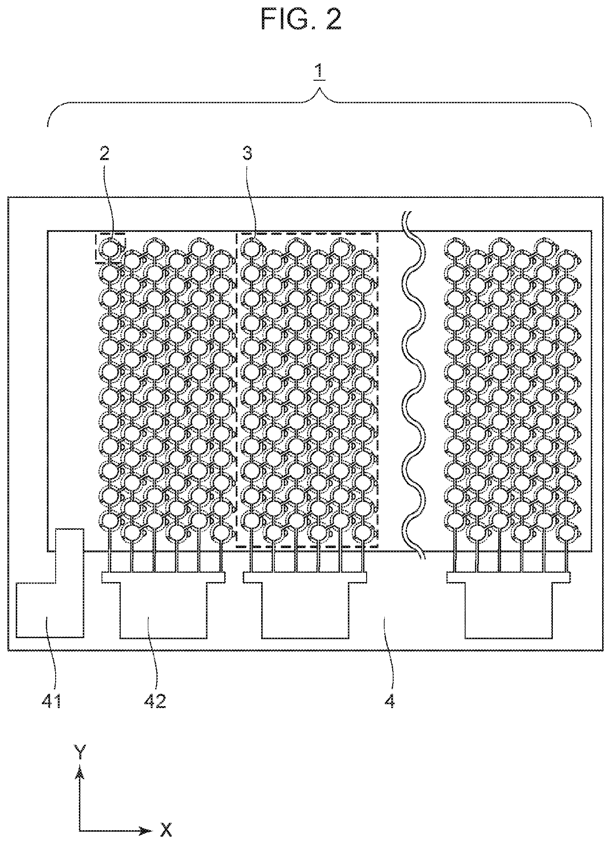
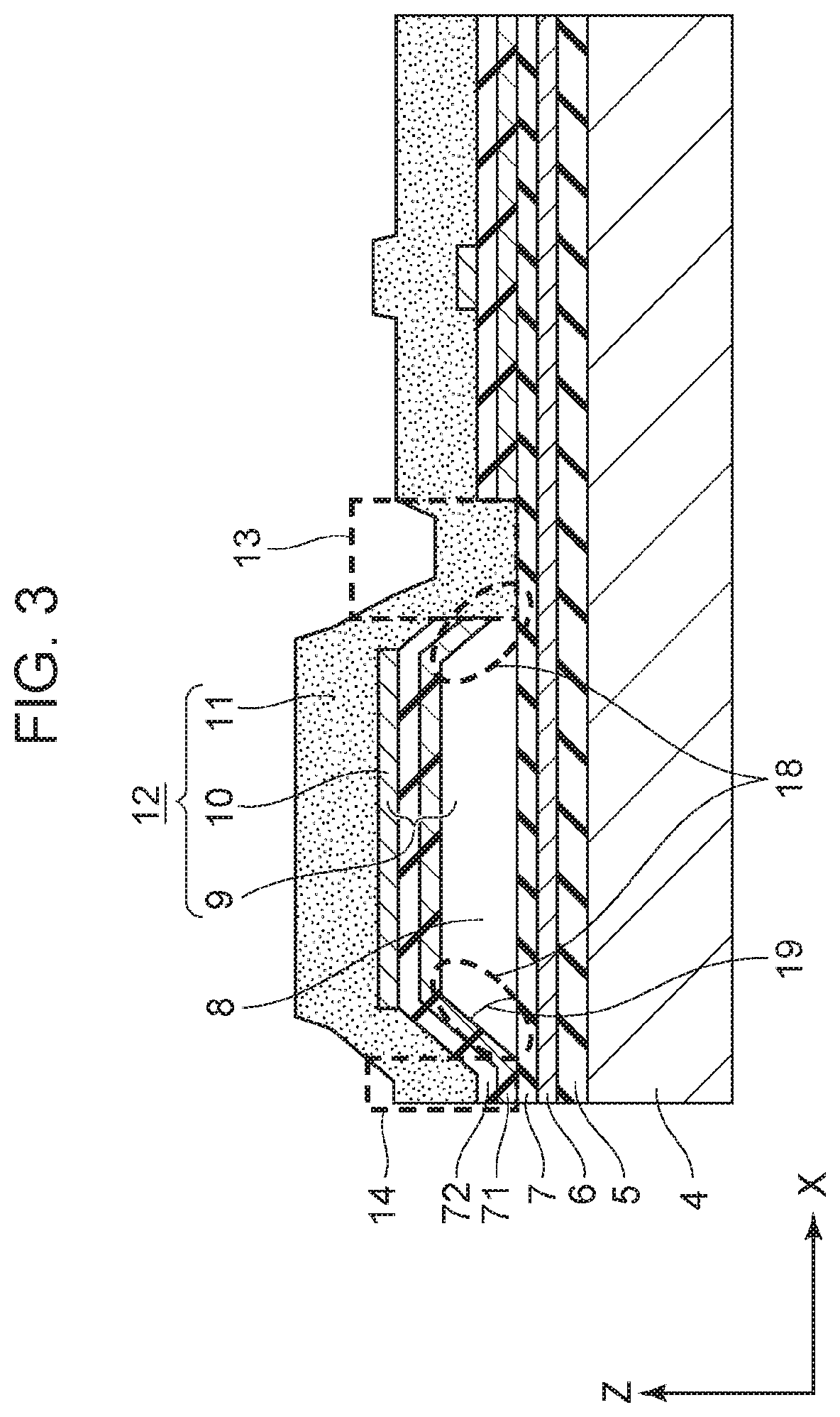
[0111]In Examples, the structure of a CMUT 1 and the method for producing a CMUT 1 will be described to show the advantageous effects of the present invention. Comparative Examples will also be described. A CMUT 1 in this Example will be described with reference to FIG. 1, FIG. 2, FIG. 18, and FIG. 19. FIG. 19 is a sectional view taken along line A-B in FIG. 1 in which a fourth insulating film 56 is further disposed.
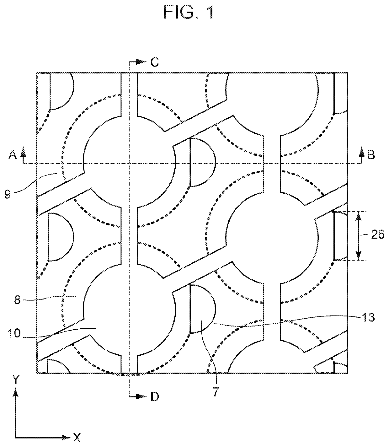
[0112]The external dimensions of the CMUT 1 illustrated in FIG. 2 are 12 (mm) in the Y direction and 45 (mm) in the X direction. The external dimensions of each of the elements 3 is 0.3 (mm) in the X direction and 4 (mm) in the Y direction, and 196 elements 3 are arranged in a one-dimensional array. FIG. 18G is a sectional view taken along line A-B in FIG. 1. Each of the cells 2 constituting the elements 3 has a substantially circular shape except for the etching opening 17, and the hollow portion 8 has a diameter of 32 (μm). The diameter of the hollow portion 8 is a dia...
example 2
[0135]In Example 2, a method for producing a hollow structure in which the sacrificial layer is made of silicon and at least one of upper and lower films that sandwich the sacrificial layer is a silicon nitride film will be described. In Example 2, first, a structure for evaluating the characteristics of a silicon nitride film, which is illustrated in a schematic sectional view of FIG. 22, was used. The growth rate of deposits on the silicon nitride film during the sacrificial layer etching with an etching gas containing xenon difluoride and hydrogen, which is not described in Example 1, Comparative Example 1, and Comparative Example 2, was measured. In addition, the thickness decrease rate of the silicon nitride film itself, that is, the etching rate was measured by providing levels having different Si / N composition ratios.
[0136]As illustrated in the sectional view before etching in FIG. 22, silicon nitride films with levels having different Si / N composition ratios were formed as a...
PUM
| Property | Measurement | Unit |
|---|---|---|
| refractive index | aaaaa | aaaaa |
| thickness | aaaaa | aaaaa |
| pressure | aaaaa | aaaaa |
Abstract
Description
Claims
Application Information