Array substrate, display panel, and display

a technology of array substrate and display panel, applied in the field of array substrate, can solve problems affecting the display quality of the panel, and achieve the effects of ensuring the display effect of the display area of the array substrate, preventing the chip-on-film connection line of the non-display area from being corroded, and preventing further penetration of water vapor into the display area

Inactive Publication Date: 2020-04-23
CHONGQING HKC OPTOELECTRONICS TECH CO LTD +1
View PDF0 Cites 6 Cited by
  • Summary
  • Abstract
  • Description
  • Claims
  • Application Information

AI Technical Summary

Benefits of technology

[0034]In the display provided by one embodiment of the present application, the chip-on-film connection line of the non-display area comprises: the first metal layer arranged on the substrate base layer, the insulation layer arranged on the first metal layer, the second metal layer arranged on the insulation layer, and the passivation layer arranged on the second metal layer; and the surface of the passivation layer is provided with the hydrophobic layer. The hydrophobic layer is capable of effectively preventing the water vapor from penetrating into the second metal layer arranged beneath the passivation layer, therefore further preventing the chip-on-film connection line of the non-display area from being corroded and preventing further penetration of the water vapor into the display area. In this way, the display effect of the display area of the array substrate is ensured, the qualities of the display panel and the display are ensured, and service lives thereof are improved.

Problems solved by technology

It is easy for the water vapor to penetrate into the second metal layer 1122′ due to environmental changes, and the water vapor entering the array substrate 100′ results in bubbles, so that the WOA line 112′ or even the array substrate 100′ is then seriously corroded, affecting the display quality of the panel.

Method used


Image

  • Array substrate, display panel, and display
  • Array substrate, display panel, and display
  • Array substrate, display panel, and display

Examples


first embodiment

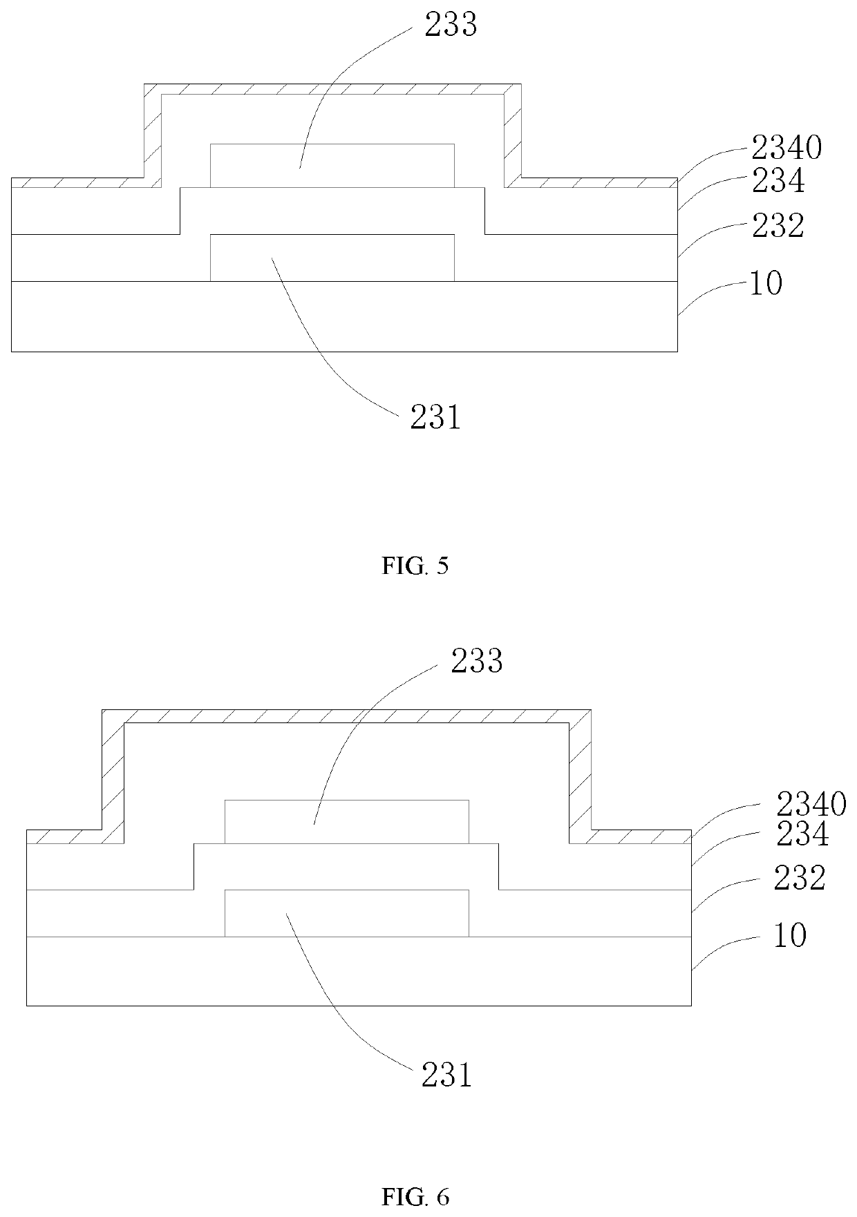
[0051]In the present application, as shown in FIG. 5, the passivation layer 234 is made from an inorganic material of silicon oxide (SiOx) or silicon nitride (SiNx), and the passivation layer 234 has a thickness of 200-230 nm. In particular, the passivation layer 234 is treated with fluoride ions to form a hydrophobic layer 2340 on a surface of the passivation layer 234. Specific steps are as follows: ionizing a gas mixture obtained by mixing CF4 or SF6 with O2, performing dry etching on the surface of the passivation layer 234 of the inorganic material by an ionized gas mixture, and forming hydrophobic groups on the surface of the passivation layer 234 to obtain the hydrophobic layer 2340.

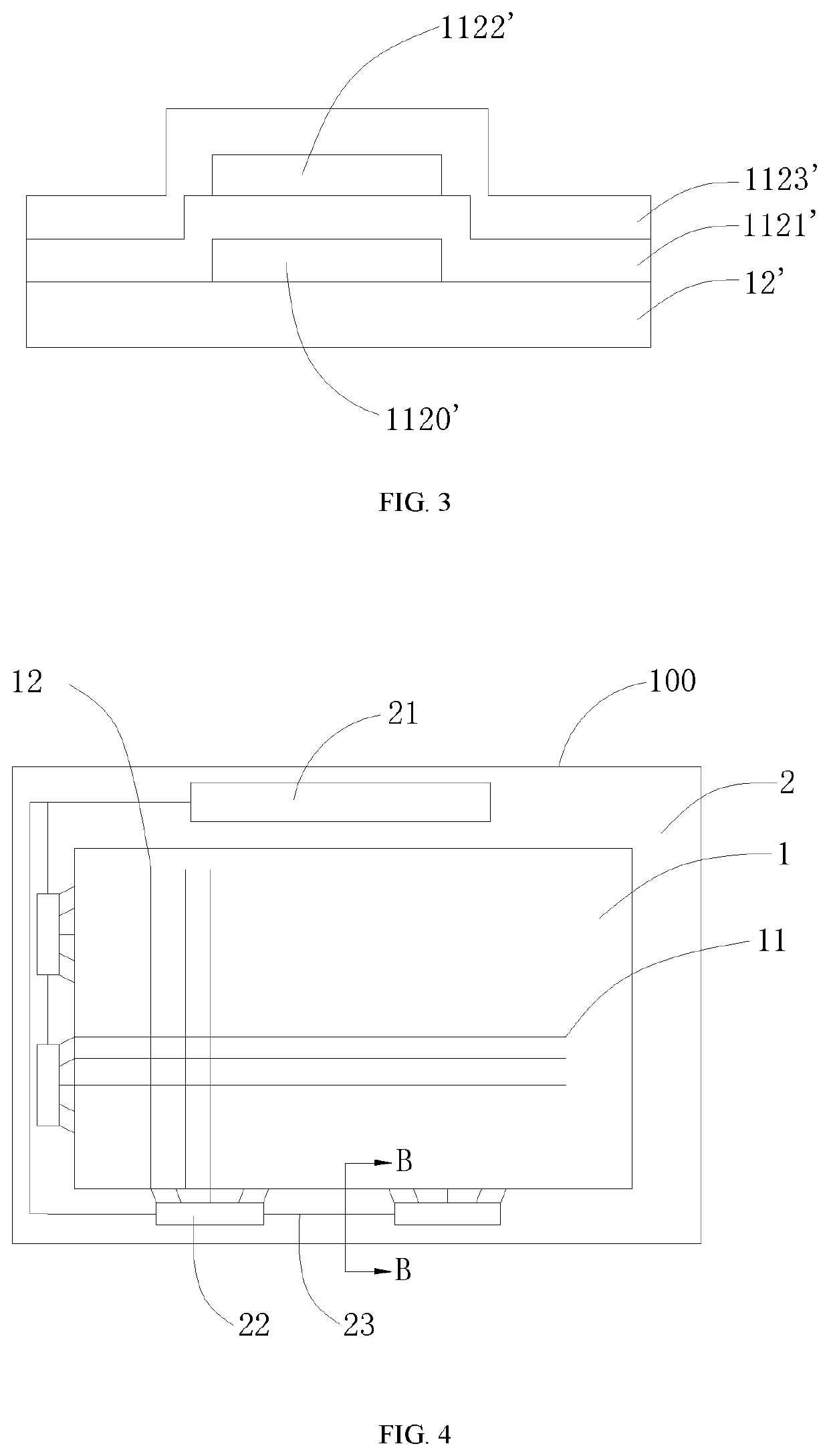
[0052]For the display area 1, a gate and the scan lines 11 are formed on the substrate base layer 10, a gate insulating layer is formed on the gate and the scan lines, an active layer is formed on the gate insulating layer, a source / drain and the data lines 12 are formed on the active layer, the g...

second embodiment

[0055]In the second embodiment, the thickness of the passivation layer 234 in the non-display area 2 is greater than that of the passivation layer on the TFT within the display area 1. In this case, after a passivation layer having a thickness of greater than 230 nm is formed by one time chemical vapor deposition, a portion of the passivation layer on the TFT within the display area can be removed. Thus, not only is the thickness of the passivation layer 234 of the chip-on-film connection line 23 maintained greater than 230 nm, but also the passivation layer on the TFT within the display area 1 is maintained at 200-230 nm.

third embodiment

[0056]In the present application, as illustrated in FIG. 7, the passivation layer 234 comprises a first sub-passivation layer 2341 disposed on the second metal layer 233 and a second sub-passivation layer 2234 disposed on the first sub-passivation layer 2341. A hydrophobic layer 2340 is formed on the surface of the second sub-passivation layer 2342. The sum of the thicknesses of the first sub-passivation layer 2341 and the second sub-passivation layer 2342 is greater than 230 nm.

[0057]In particular, the first sub-passivation layer 2341 has a thickness of 200-230 nm, and the second sub-passivation layer 2342 has a thickness of smaller than 230 nm, for example, smaller than 70 nm, 70-170 nm, or alternatively, 170-230 nm, and the thickness of the passivation layer 234 is 230-460 nm.

[0058]Optionally, the first passivation layer 2341 is made from an inorganic material of silicon oxide (SiOx) or silicon nitride (SiNx), and the second passivation layer 2342 is made from an organic material...


PUM

PropertyMeasurementUnit
thicknessaaaaaaaaaa
thicknessaaaaaaaaaa
thicknessaaaaaaaaaa

Abstract

An array substrate (100) provided by an embodiment of the present application including a chip-on-film connection line (23). The chip-on-film connection line (23) includes: a first metal layer (231), an insulation layer (232), a second metal layer (233), and a passivation layer (234). A surface of the passivation layer (234) has a hydrophobic layer (2340).

Description

CROSS-REFERENCE TO RELATED APPLICATIONS[0001]This application is the International Application No. PCT / CN2018 / 111486 for entry into US national phase with an international filing date of Oct. 23, 2018, designating US, now pending, and claims priority to Chinese Patent Application No. 201811012705.X, filed on Aug. 31, 2018, the content of which is incorporated herein by reference in its entirety.BACKGROUND OF THE INVENTIONField of the Invention[0002]The present application relates to the technical field of display technologies, and more particularly to an array substrate, a display panel, and a display.Description of Related Art[0003]A Liquid Crystal Display (LCD) is a commonly used electronic device and is widely favored by users due to its low power consumption, small size, and light weight. The current liquid crystal display device is mainly a thin film transistor (TFT) liquid crystal display (TFT-LCD).[0004]The liquid crystal display mainly includes a liquid crystal display panel...

Claims


Application Information

Patent Timeline
Patent Type & Authority Applications(United States)
IPC IPC(8): H01L27/12H01L23/00G02F1/1362G02F1/1345G02F1/1339G02F1/1333
CPCH01L27/1244H01L27/1248H01L23/564G02F2201/501G02F1/13452G02F1/1339G02F1/133345G02F1/136286G02F1/1362G02F1/1345G02F1/13629H01L27/124
Inventor YANG, YANNA
Owner CHONGQING HKC OPTOELECTRONICS TECH CO LTD
Why Eureka
Try Eureka