

Semiconductor device and power converter
- Summary
- Abstract
- Description
- Claims
- Application Information
AI Technical Summary
Benefits of technology
Problems solved by technology
Method used
Image

Examples
embodiment 1
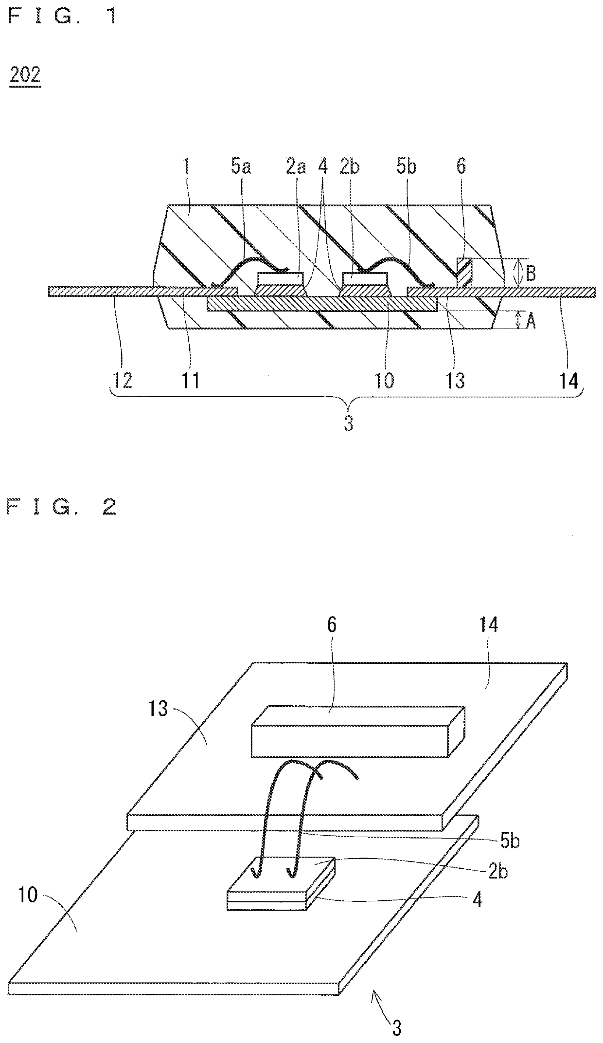
[0020]Embodiment 1 of the present invention will be described below with use of the drawings. FIG. 1 is a sectional view of an essential part of a semiconductor device 202 according to Embodiment 1. FIG. 2 is a perspective view of a semiconductor element 2b and a resin wall 6 disposed on an upper surface of a lead frame 3 included in the semiconductor device 202.
[0021]As illustrated in FIG. 1, the semiconductor device 202 is a semiconductor power module widely used in consumer appliances, industry, automobiles, and trains, for example. The semiconductor device 202 includes a sealing resin 1, semiconductor elements 2a and 2b, the lead frame 3, a bonding material 4, wires 5a and 5b, and the resin wall 6.
[0022]The semiconductor elements 2a and 2b are power semiconductor elements operating at 150° C. or more, for example, and are mounted over an upper surface of a mount 10 of the lead frame 3 via the bonding material 4. The semiconductor elements 2a and 2b may each include a so-called w...
embodiment 2
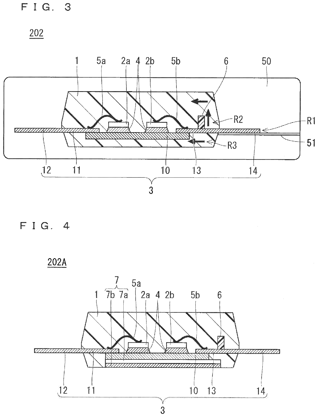
[0047]A semiconductor device according to Embodiment 2 will be described next. FIG. 4 is a sectional view of an essential part of the semiconductor device according to Embodiment 2. In Embodiment 2, the same components as those described in Embodiment 1 bear the same reference signs as those in Embodiment 1, and description thereof is omitted.
[0048]As illustrated in FIG. 4, a semiconductor device 202A further includes an insulating sheet 7 disposed at the lower end of the lead frame 3 in Embodiment 2. The insulating sheet 7 is bonded to the lower end of the lead frame 3, that is, to the lower surface of the mount 10 of the lead frame 3, and is provided to secure high insulation and heat dissipation of the mount 10 of the lead frame 3. The insulating sheet 7 includes a sheet layer 7a having insulation and a metal plate 7b. The sheet layer 7a is made of a cured resin in which ceramic powder is dispersed or a cured resin in which a ceramic plate is buried. The sheet layer 7a is bonded ...
embodiment 3
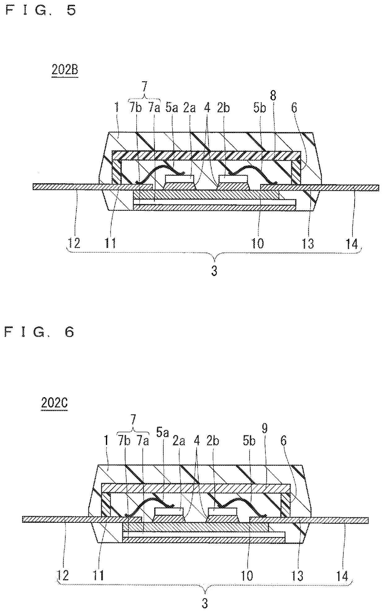
[0055]A semiconductor device according to Embodiment 3 will be described next. FIG. 5 is a sectional view of an essential part of a semiconductor device 202B according to Embodiment 3. In Embodiment 3, the same components as those described in Embodiments 1 and 2 bear the same reference signs as those in Embodiments 1 and 2, and description thereof is omitted.
[0056]As illustrated in FIG. 5, in Embodiment 3, the semiconductor device 202B includes two resin walls 6. One of the resin walls 6 is provided on the inner lead 13 between the outer lead 14 and the mount 10 of the lead frame 3 on one side. The other one of the resin walls 6 is provided on the inner lead 11 between the outer lead 12 and the mount 10 of the lead frame 3 on the other side. The semiconductor device 202B further includes a resin plate 8 connecting upper end portions of the two resin walls 6 with each other. The two resin walls 6 and the resin plate 8 are sealed by the sealing resin 1.
[0057]In the related technology...
PUM
 Abstract
Description
Claims
Application Information