Monolithic qubit integrated circuits

a monolithic, integrated circuit technology, applied in the field of integrated circuits, can solve the problems of limited operation, lack of monolithic integration, degrade readout fidelity and computing speed, etc., to avoid overloading qubits and maximize spin-readout bandwidth

a monolithic, integrated circuit technology, applied in the field of integrated circuits, can solve the problems of limited operation, lack of monolithic integration, degrade readout fidelity and computing speed, etc., to avoid overloading qubits and maximize spin-readout bandwidth

US20200185512A1Active Publication Date: 2020-06-11THE GOVERNINIG COUNCIL OF THE UNIV OF TORANTO

Image

  • Monolithic qubit integrated circuits
  • Monolithic qubit integrated circuits
  • Monolithic qubit integrated circuits

Examples


Embodiment Construction

[0062]The description that follows, and the embodiments described therein, are provided by way of illustration of an example, or examples, of particular embodiments of the principles of the present invention. These examples are provided for the purposes of explanation, and not of limitation, of those principles and of the invention. In the description, like parts are marked throughout the specification and the drawings with the same respective reference numerals. The drawings are not necessarily to scale and in some instances proportions may have been exaggerated in order to more clearly to depict certain features of the invention.

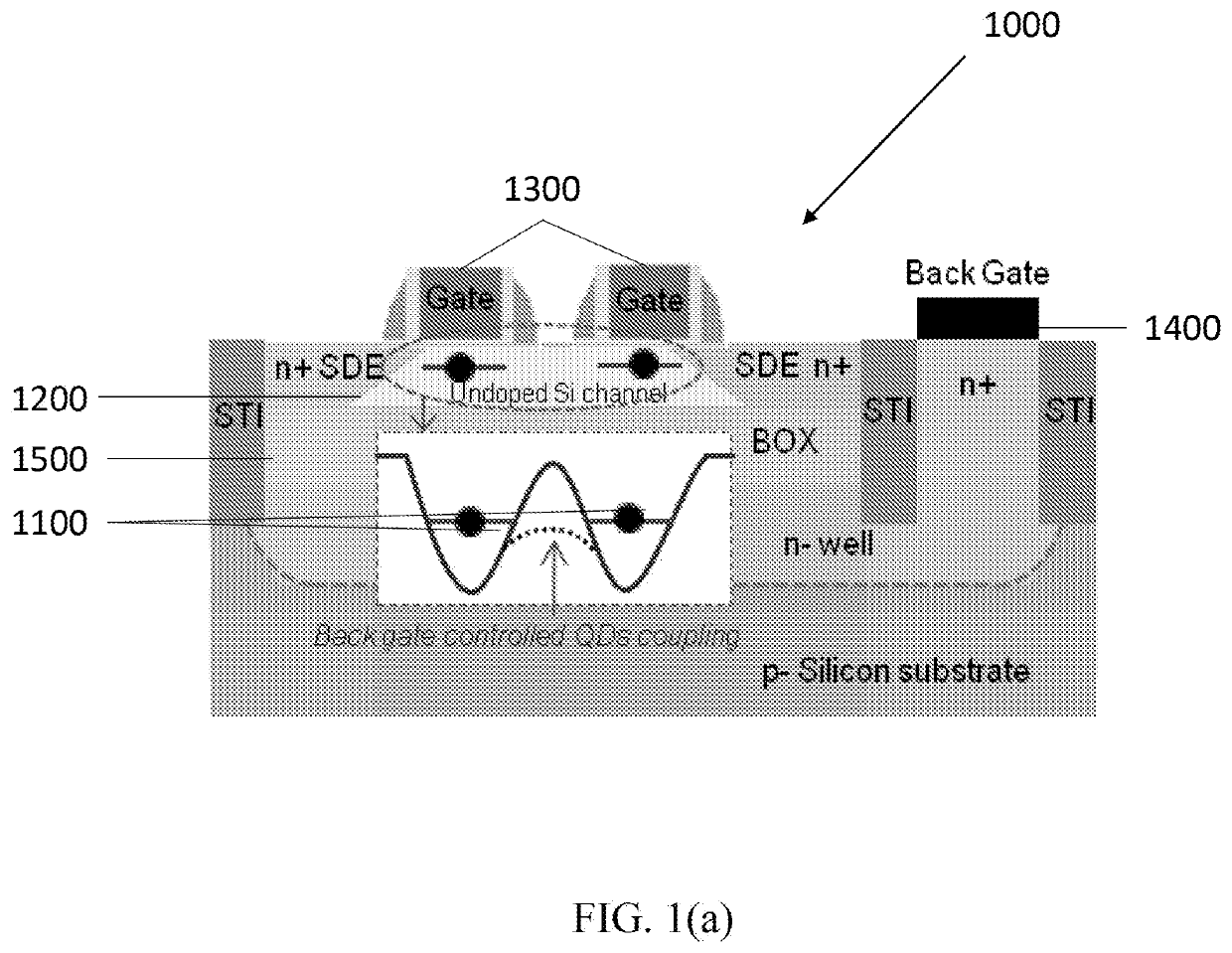
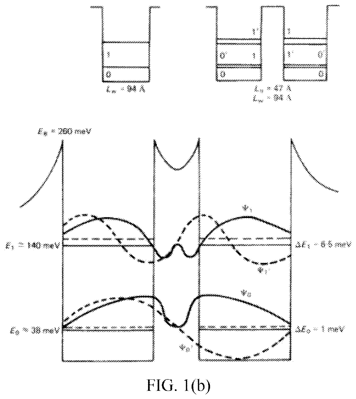
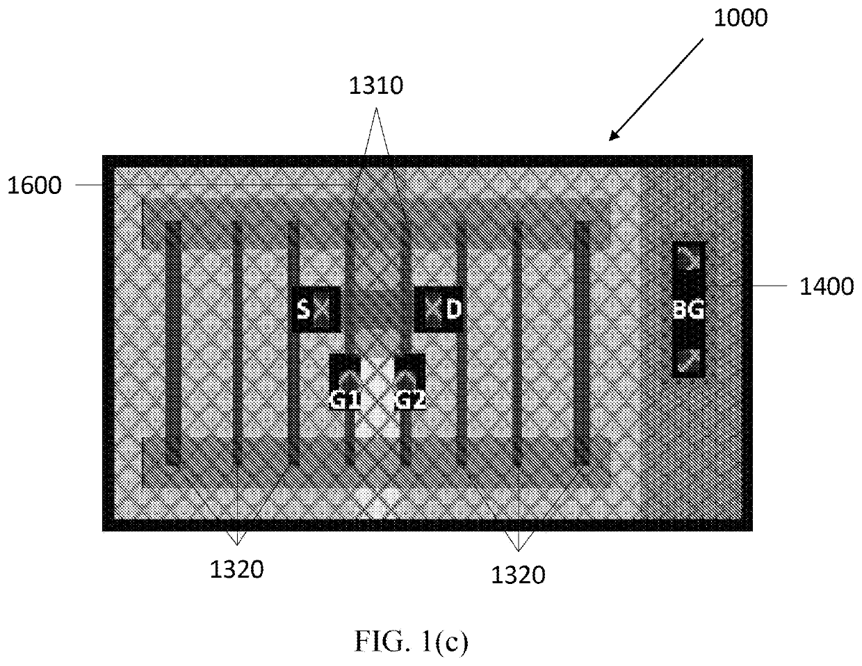
[0063]According to an embodiment, this description relates to monolithically integrated semiconductor quantum processors, such as per the characterizations in D1 (S. Bonen, et al. Cryogenic Characterization of 22-nm FDSOI CMOS Technology for Quantum Computing ICs. In IEEE, 2018) and the designs in D2 (M Gong, et al. Design Considerations for Spin Readout A...


PUM


Abstract

Described is a monolithic integrated circuit for use in quantum computing based on single and multiple coupled quantum dot electron- and hole-spin qubits monolithically integrated with the mm-wave spin manipulation and readout circuitry in commercial complementary metal-oxide-semiconductor (CMOS) technology. The integrated circuit includes a plurality of n-channel or p-channel metal-oxide-semiconductor field-effect transistor (MOSFET) cascodes each including a single-spin qubit or two coupled quantum dot qubits formed in an undoped semiconductor film adjacent at least one top gate. There is also a back gate formed in a silicon substrate adjacent a buried oxide layer or the at least one top gate, where the back gate controls the electron or hole entanglement and exchange interaction between the two coupled quantum dot qubits. The monolithic integrated circuits described may be used for monolithically integrated semiconductor quantum processors for quantum information processing.

Description

FIELD OF THE INVENTION[0001]The present specification relates generally to integrated circuits (ICs) and more specifically to monolithically integrated semiconductor quantum processors.BACKGROUND OF THE INVENTION[0002]Silicon-based electron-spin and hole-spin coupled quantum-dot (QD) qubits have attracted substantial interest due to their potential for integration in commercial complementary metal-oxide-semiconductor (CMOS) technology. However, because of the low confinement and coupling energies (e.g., ΔE, in the tens of μeV range, comparable to the thermal noise level, kBT, at 100 mK) their operation has been restricted to temperatures below 100 mK.[0003]The current approach is for qubit array chips to be separately packaged and operated at a base temperature below 100 mK with their microwave control and readout electronics located on a separate die at 1-4 K and accessed via a large number of 50Ω coaxial cables. However, the lack of monolithic integration degrades readout fidelity...

Claims


Application Information

Patent Timeline
11 Jun 2020
Publication
US20200185512A1
IPC
H01L29/66; G06N10/00; H01L27/06
CPC
G06N10/00; H01L29/66984; H01L27/0629; H01L29/66977; H01L21/823437; H01L27/1203; H01L29/78648; B82Y10/00
Inventors
VOINIGESCU, SORIN PETRE; ALAKUSU, UTKU