Display device and electronic device

a technology of electronic devices and display devices, applied in static indicating devices, instruments, optics, etc., can solve the problems of delay in displaying images, increased circuit scale and power consumption of equipment, and sometimes too much processing, etc., and achieves low power consumption and high reliability.

Active Publication Date: 2020-06-18
SEMICON ENERGY LAB CO LTD
View PDF0 Cites 24 Cited by
  • Summary
  • Abstract
  • Description
  • Claims
  • Application Information

AI Technical Summary

Benefits of technology

[0027]Alternatively, it is possible to provide a display device with low power consumption, a highly reliable display device, a novel display device or the like, a method for driving any of the above display devices, or a novel semiconductor device or the like.

Problems solved by technology

Equipment performing image correction analyzes an enormous amount of image data and produces new image data; thus, the circuit scale and power consumption of the equipment are increased.
Moreover, the amount of processing is sometimes too much to handle in real time, causing a delay in displaying images.

Method used


Image

  • Display device and electronic device
  • Display device and electronic device
  • Display device and electronic device

Examples


embodiment 1

[0054]In this embodiment, a display device that is one embodiment of the present invention will be described with reference to drawings.

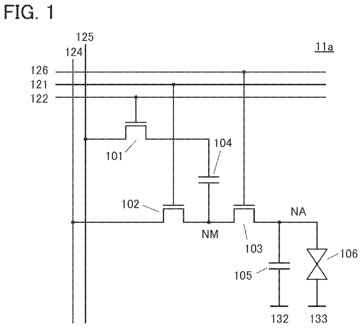
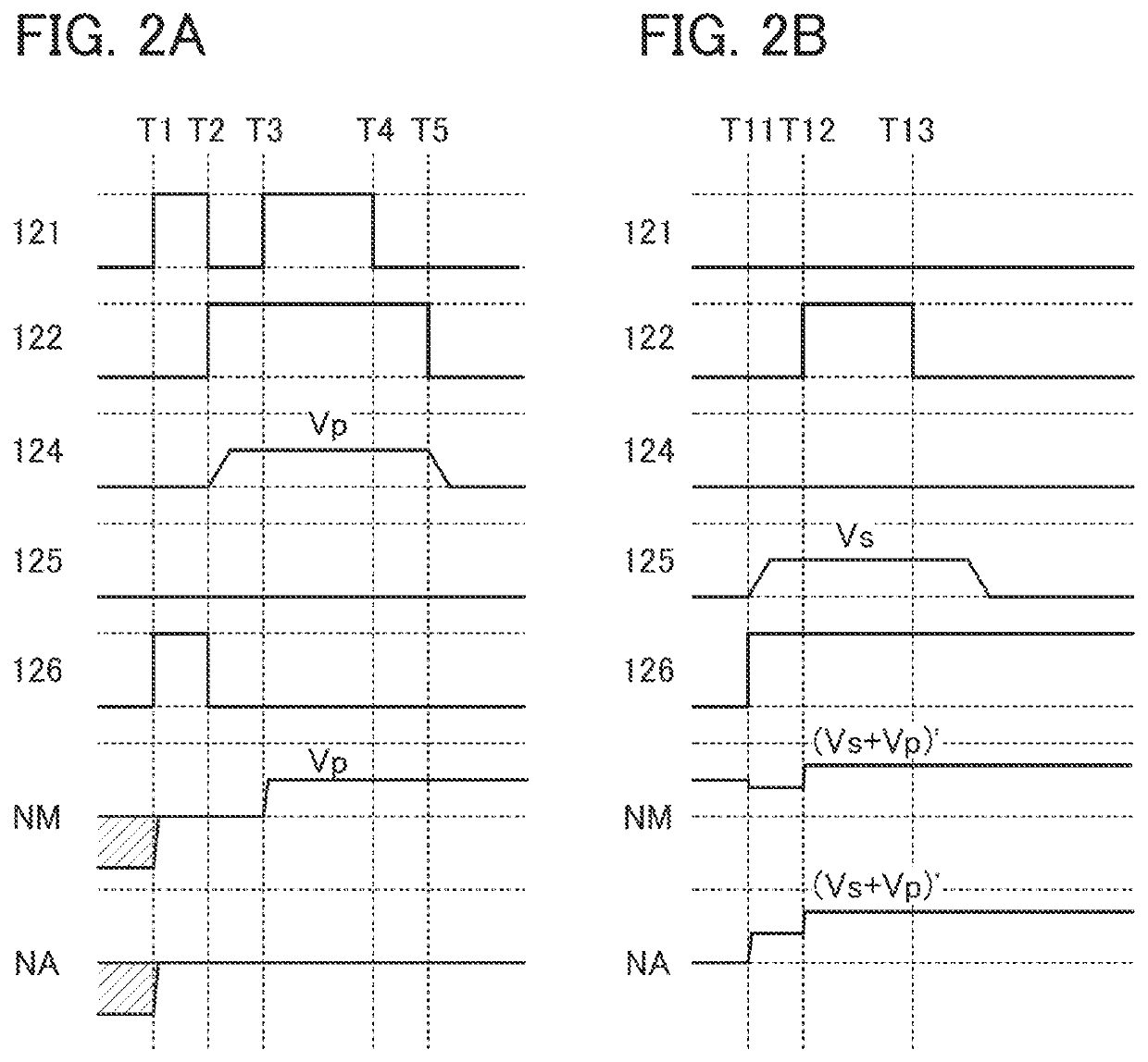
[0055]One embodiment of the present invention is a display device having a function of adding correction data to image data. A memory node is provided in each pixel, and intended correction data is held in the memory node. The correction data is produced in an external device and written into each pixel.

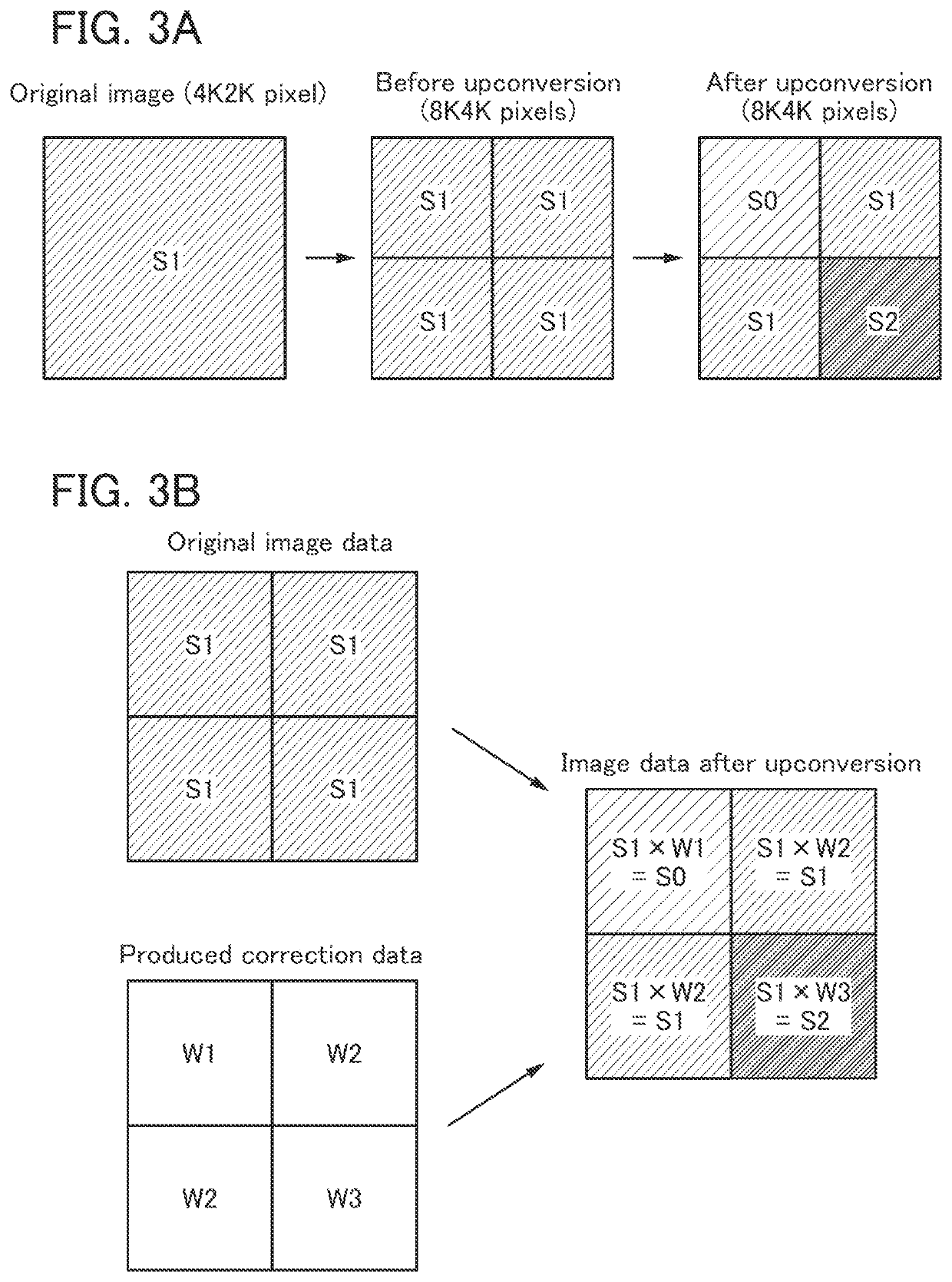
[0056]The correction data is added to image data owing to capacitive coupling, and the resulting data is supplied to a display element. Thus, a corrected image can be displayed with the display element. The correction performed in this manner enables image upconversion, for example, or can compensate for an image quality reduction due to characteristics variations of transistors included in the pixels.

[0057]FIG. 1 illustrates a pixel 11a that can be used for the display device of one embodiment of the present invention. The pixel 11a includes a trans...

embodiment 2

[0193]In this embodiment, structure examples of a display device including a liquid crystal element will be described. Note that the operation and the functions for the correction described in Embodiment 1 are not repeatedly described in this embodiment.

[0194]FIGS. 13A to 13C are diagrams each illustrating a structure of a display device to which one embodiment of the present invention can be applied.

[0195]In FIG. 13A, a sealant 4005 is provided so as to surround a display portion 215 provided over a first substrate 4001, and the display portion 215 is sealed by the sealant 4005 and a second substrate 4006.

[0196]A pixel array including the pixels described in Embodiment 1 is provided in the display portion 215.

[0197]In FIG. 13A, each of a scan line driver circuit 221a, a signal line driver circuit 231a, a signal line driver circuit 232a, and a common line driver circuit 241a includes a plurality of integrated circuits 4042 provided over a printed circuit board 4041. The integrated c...

embodiment 3

[0240]In this embodiment, an example of a transistor that can be used as the transistors described in the above embodiments will be described with reference to drawings.

[0241]The display device of one embodiment of the present invention can be fabricated using a transistor with any of various modes, such as a bottom-gate transistor or a top-gate transistor. Therefore, a material for a semiconductor layer or the structure of a transistor can be easily changed depending on the existing production line.

[Bottom-Gate Transistor]

[0242]FIG. 16A1 is a cross-sectional view of a channel-protective transistor 810 that is a type of bottom-gate transistor. In FIG. 16A1, the transistor 810 is formed over a substrate 771. The transistor 810 includes an electrode 746 over the substrate 771 with an insulating layer 772 therebetween. The transistor 810 includes a semiconductor layer 742 over the electrode 746 with an insulating layer 726 therebetween. The electrode 746 can serve as a gate electrode. ...


PUM

PropertyMeasurementUnit
energy gapaaaaaaaaaa

Abstract

A display device capable of performing image processing is provided. A memory node is provided in each pixel included in the display device. An intended correction data is held in the memory node. The correction data is calculated by an external device and written into each pixel. The correction data is added to image data by capacitive coupling, and the resulting data is supplied to a display element. Thus, the display element can display a corrected image. The correction enables image upconversion, for example.

Description

TECHNICAL FIELD[0001]One embodiment of the present invention relates to a display device.[0002]Note that one embodiment of the present invention is not limited to the above technical field. The technical field of one embodiment of the invention disclosed in this specification and the like relates to an object, a method, or a manufacturing method. Furthermore, one embodiment of the present invention relates to a process, a machine, manufacture, or a composition of matter. Specific examples of the technical field of one embodiment of the present invention disclosed in this specification include a semiconductor device, a display device, a liquid crystal display device, a light-emitting device, a lighting device, a power storage device, a memory device, an imaging device, a method for driving any of them, and a method for manufacturing any of them.[0003]In this specification and the like, a semiconductor device generally means a device that can function by utilizing semiconductor charac...

Claims


Application Information

Patent Timeline
Patent Type & Authority Applications(United States)
IPC IPC(8): G09G3/36H01L27/105H01L27/12H01L29/24H01L29/786G02F1/1368G02F1/1362
CPCG09G2300/0842H01L29/78648H01L27/124H01L27/1052H01L27/1225H01L29/24G02F2001/13685G02F1/1368H01L27/1207G09G3/3685H01L29/7869G09G2320/02G02F1/13624H01L29/78633H01L27/1255G09G3/3659G09G3/3677G09G3/3688G09G2300/0426G09G2300/0852G09G2310/08G09G2340/0414G09G2340/0421G09G2340/0428G02F1/13338G02F1/136213G06F1/1652H01L29/78645H01L27/0688H01L29/786G02F1/133G02F1/1343G02F1/13685H10B99/00
Inventor KAWASHIMA, SUSUMUKUSUNOKI, KOJIWATANABE, KAZUNORITOYOTAKA, KOUHEIKUSUMOTO, NAOTOYAMAZAKI, SHUNPEI
Owner SEMICON ENERGY LAB CO LTD
Why Eureka
Try Eureka