Method for bonding and interconnecting semiconductor chips

a technology of interconnection and semiconductor chips, which is applied in the direction of semiconductor/solid-state device manufacturing, electric devices, solid-state devices, etc., can solve the problems of difficult to obtain a very flat surface, inferior quality of bonding, and error in the alignment of metal pads

Active Publication Date: 2020-06-25
INTERUNIVERSITAIR MICRO ELECTRONICS CENT (IMEC VZW)
View PDF0 Cites 3 Cited by
  • Summary
  • Abstract
  • Description
  • Claims
  • Application Information

AI Technical Summary

Benefits of technology

[0007]A method is provided that suffers from neither of the above-described disadvantages. This aim is achieved by the methods disclosed in the appended claims. The embodiments are related to a method for bonding and interconnecting two semiconductor chips arranged on substrates such as silicon wafers. The embodiments take advantage of a number of known characteristics of the class of compounds known as Hydrogen Silsesquioxane (HSQ) and materials equivalent to HSQ, in order to solve the above shortcomings of the prior art. HSQ or its equivalent is used as a bonding layer for bonding two device wafers, and

Problems solved by technology

Option 1 (dielectric bonding) is challenging for TSV processing by lithography and etching, since it requires the etch to be compatible with both types of TSV (deep and shallow) or if this is not possible, the approach requires different reticles, which is costly.
Option 2 (hybrid bonding) is challenging from the bonding perspective since two different materials are present at the interface: metal and dielectric.
This may cause

Method used


Image

  • Method for bonding and interconnecting semiconductor chips
  • Method for bonding and interconnecting semiconductor chips
  • Method for bonding and interconnecting semiconductor chips

Examples


Embodiment Construction

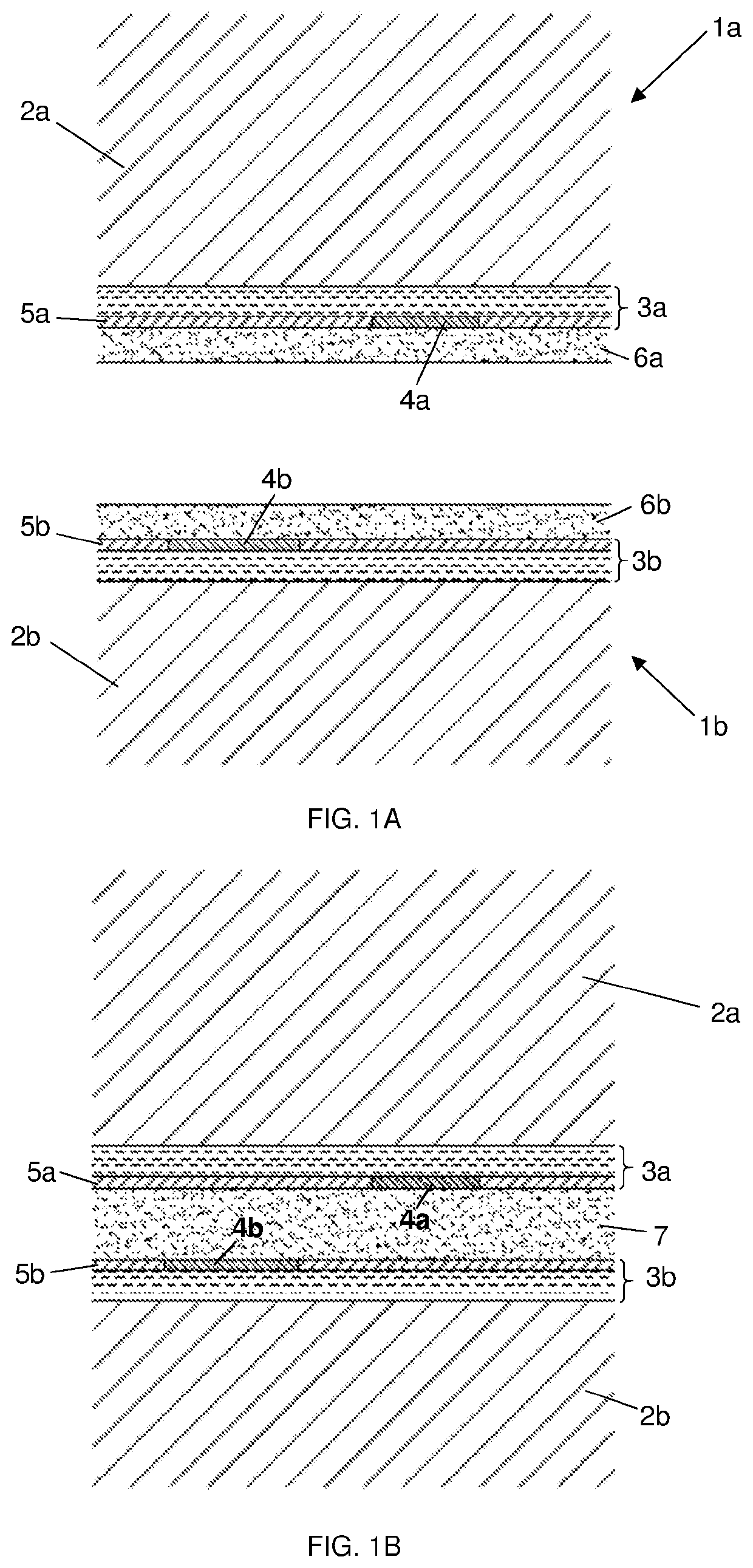
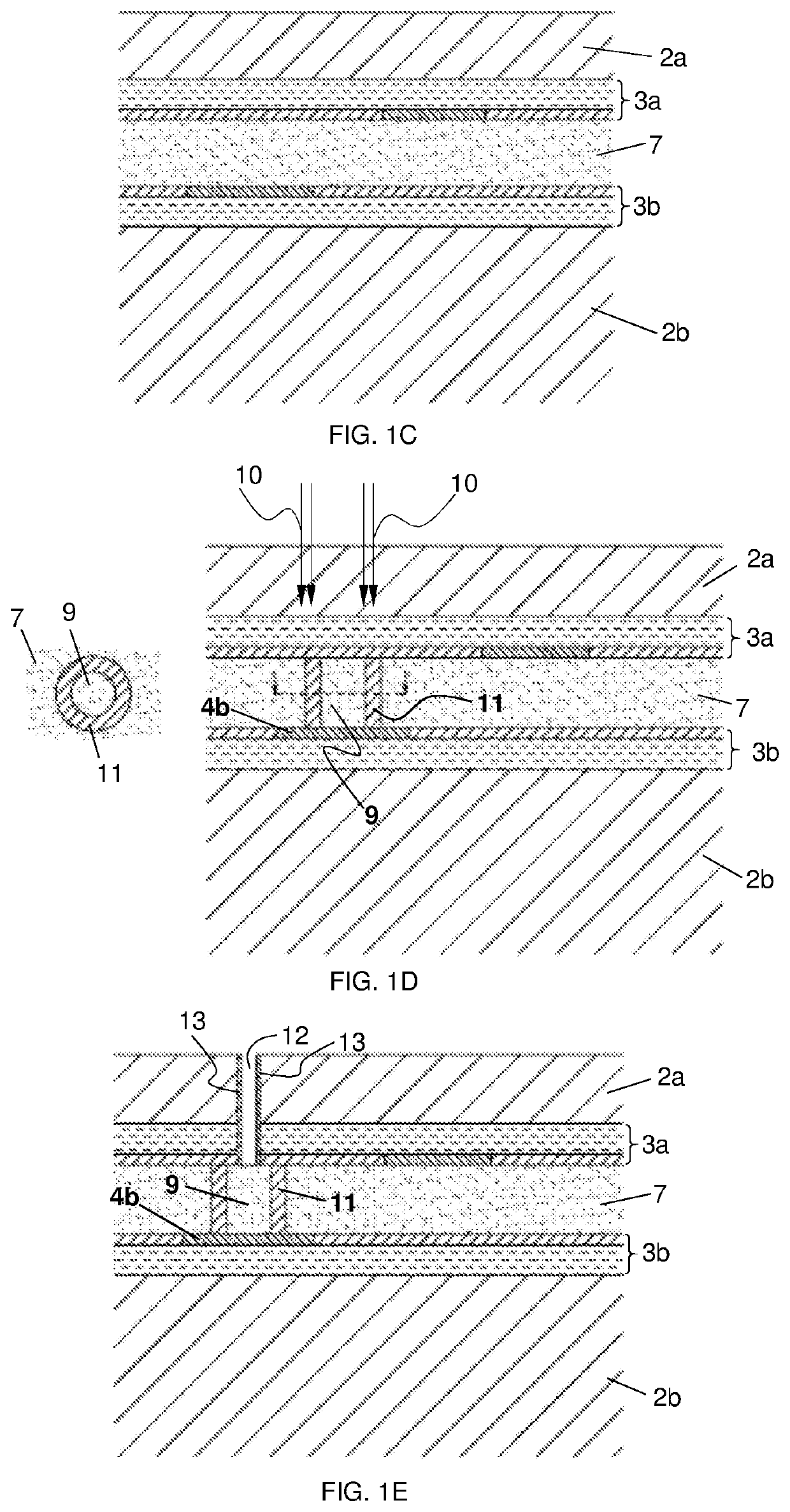
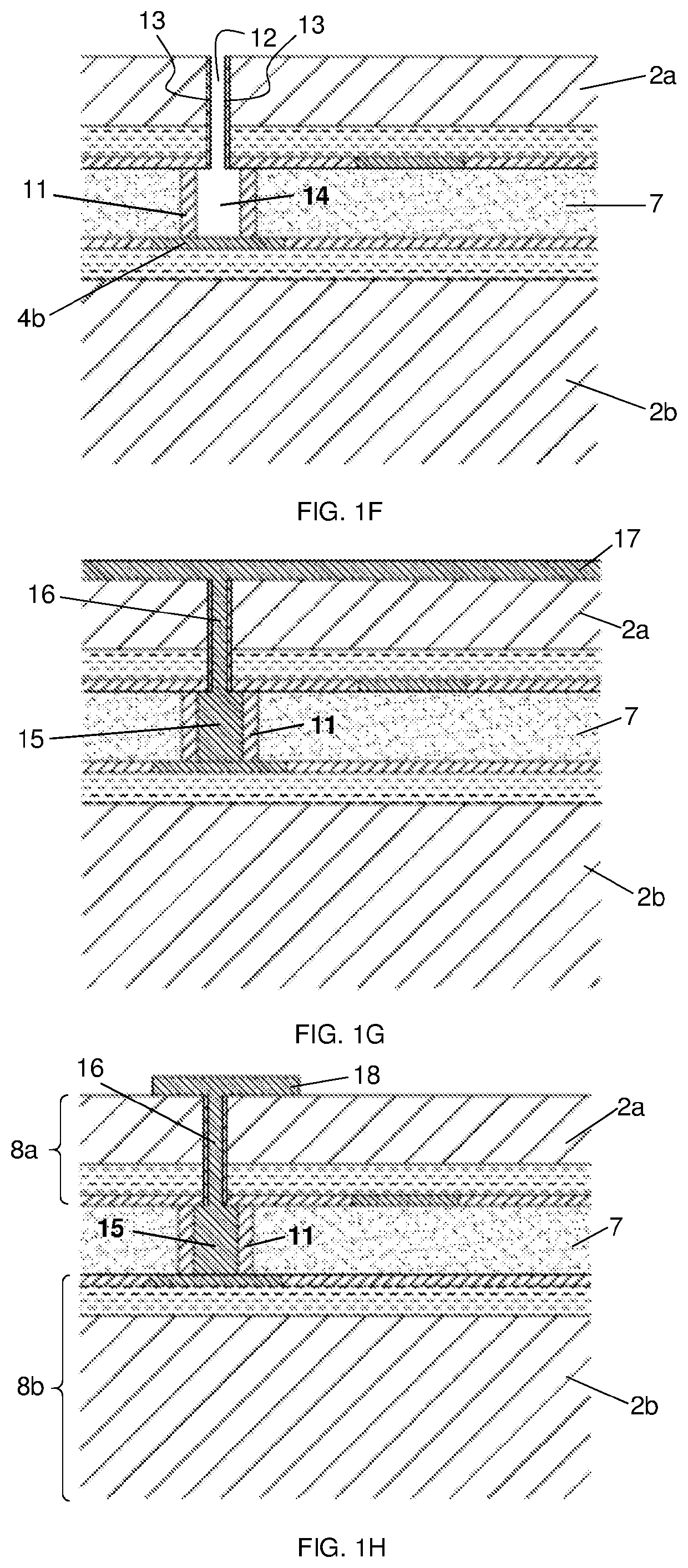
[0036]The term HSQ represents a class of inorganic compounds with the chemical formula [HSiO3 / 2]n. The variable n can be any suitable integer, e.g., an integer of 10 or more (e.g., 10-1000) Any compound within this class is applicable in the embodiments. Materials applicable instead of HSQ and in the same way as HSQ are partially condensed silsesquioxanes in which 2 or more long chains of RSiO3 / 2 units are connected at regular intervals by Si—O—Si bonds, where R can be a hydrogen atom, an alkyl, an aryl or an alkoxy functional group. In certain embodiments, a long chain is a chain having 10 or more (e.g., 10-1000) RSiO3 / 2 units. In certain embodiments, the alkyl is a C1-10 alkyl, the aryl is a 06-14 aryl and the alkoxy is a C1-10 alkoxy, however, in other embodiments these groups may contain a higher number of carbon atoms than specified. These alternative materials are referred to within the present context as materials “equivalent” to HSQ. The use of HSQ as a resist in e-beam lith...


PUM


Abstract

A method is provided for bonding and interconnecting two semiconductor chips arranged on semiconductor substrates. HSQ (Hydrogen Silsesquioxane) or an equivalent material is used as a bonding layer and after bonding and thinning one of the wafers (or first thinning and then bonding), the bond layer is locally irradiated by an e-beam through the thinned substrate, thereby locally transforming the bonding material into silicon oxide. Then a via opening is etched through the thinned substrate and an etch process selectively removes the oxide from an area delimited by the bonding material or vice versa. The filling of the via opening establishes an electrical connection between the bonded wafers, that is equivalent to a connection obtained by hybrid bonding, but that does not suffer from the disadvantages thereof.

Description

INCORPORATION BY REFERENCE TO RELATED APPLICATION[0001]Any and all priority claims identified in the Application Data Sheet, or any correction thereto, are hereby incorporated by reference under 37 CFR 1.57. This application claims the benefit of European Application No. EP 18213852.9, filed on Dec. 19, 2018. The aforementioned application is incorporated by reference herein in its entirety, and is hereby expressly made a part of this specification.FIELD OF THE INVENTION[0002]The 3D-integration of semiconductor integrated circuit chips, i.e. to the production of stacked interconnected chips, by bonding of device wafers is provided.STATE OF THE ART[0003]Various approaches for stacked 3D integration have been studied and developed. A favoured approach involves the bonding of fully processed device wafers followed by the formation of the electrical interconnection of the devices on the respective wafers by Through Semiconductor Via (TSV) connections formed by etching through a thinned ...

Claims


Application Information

Patent Timeline
IPC IPC(8): H01L21/768H01L23/00H01L23/538H01L25/065
CPCH01L21/76877H01L25/0657H01L24/05H01L24/94H01L21/76802H01L24/67H01L23/5384H01L2924/14H01L21/2007H01L21/76898H01L24/80H01L23/481
Inventor HIBLOT, GASPARDJUSSOT, JULIENVAN DER PLAS, GEERT
Owner INTERUNIVERSITAIR MICRO ELECTRONICS CENT (IMEC VZW)
Why Eureka
Try Eureka