
Health monitoring device

Active Publication Date: 2020-07-02
ECOLE POLYTECHNIQUE FEDERALE DE LAUSANNE (EPFL)
View PDF2 Cites 3 Cited by
  • Summary
  • Abstract
  • Description
  • Claims
  • Application Information

AI Technical Summary

Benefits of technology

The technical effect of this patent is the use of a pinned photodiode, which allows for the use of shorter illumination pulses, reducing power consumption and making the device compatible with small, lightweight devices. The signal to noise ratio is improved by eliminating the DC portion of the signal, without any need for power-hungry signal processing downstream. The subtraction process is simple and passive, maintaining power consumption at a bare minimum. This results in a significant reduction of power consumption compared to existing PPG systems, rendering them suitable to be carried and worn permanently.

Problems solved by technology

The combination of these aspects surprisingly results in massive reduction of power consumption compared to existing PPG systems, rendering them suitable to be carried and worn permanently.

Method used


Image

  • Health monitoring device
  • Health monitoring device
  • Health monitoring device

Examples


first embodiment

[0122]A first embodiment relates to a single transfer gate pixel arrangement.

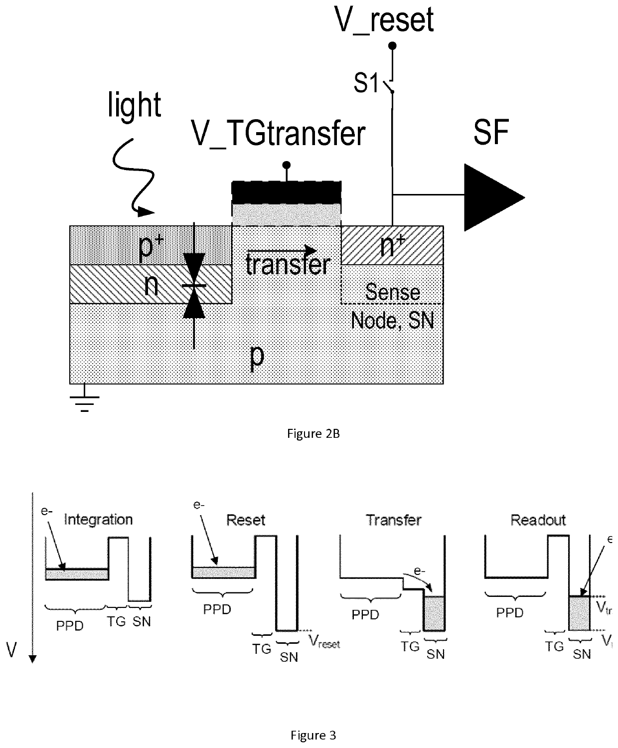
[0123]A PPD comprises a p+-n-p junction (n-p junction buried under a shallow highly doped p+), as shown in FIG. 2B which illustrates a first embodiment of a pixel. The substrate in which the PPD is formed is of p-type doped semiconductor material, and is grounded, leaving the p+ doped zone essentially floating. This forms a charge well in which photogenerated charge accumulates, increasing the voltage at the p+ layer as the charge accumulates. In essence, the p+-n-p doped structure formed in the thickness of the substrate essentially forms two diodes arranged cathode-to-cathode, then layer being shared between both, as illustrated schematically by means of the two nose-to-nose diode symbols on FIG. 2B (note: this symbol is schematic and does not indicate extra components, and merely illustrates the function of the layers and their junctions). This nose-to-nose diode symbol is unconventional, and has been us...

second embodiment

[0159]A second embodiment relates to a dual transfer gates pixel arrangement.

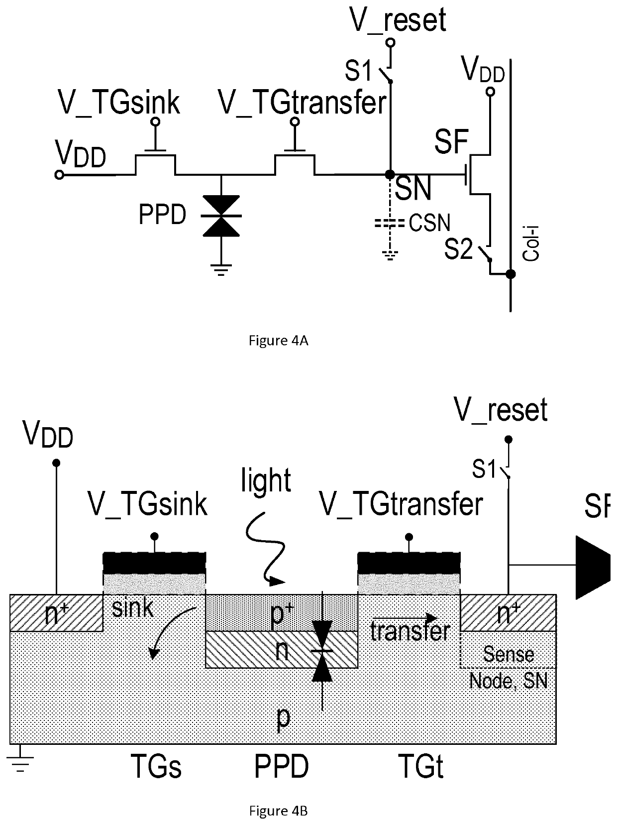
[0160]Further to the first embodiment, it is proposed here a pixel arrangement where, instead of having the PPD electronically connected to the TGtransfer transistor and the ground like in the previous embodiment, at each pixel level, the PPD is electronically connected between the TGtransfer transistor and another transistor, called TGsink transistor, that is to say two transfer gates TGt and TGs corresponding to TGtransfer transistor and TGsink transistor respectively. This is illustrated in FIG. 4A, which differs from FIG. 2A in that the PPD is additionally connected to a drain voltage VDD, which permits emptying the “well” of the PPD independently of the TGtransfer transistor. The exact geometric relationship between TGtransfer and TGsink to the p+ zone of the PPD is unimportant, provided that they can both empty the well of the PPD and do not negatively influence each other. Each transistor being situa...


PUM


Abstract

The invention relates to a photoplethysmography (PPG) sensing device comprising —a pulsed light source, —at least one pixel to create photo-generated electrons, synchronized with said pulsed light source. It is mainly characterized in that each pixel comprises: —a pinned photodiode (PPD) having two electronic connection nodes, —a sense node (SN), to convert the photo-generated electrons into a voltage, and —a Transfer Gate (TGtransfer) transistor, having its source electronically connected to one electronic connection node of said pinned photodiode (PPD), and being configured to act as a transfer gate (TG) between said pinned photodiode (PPD) and said sense node (SN), allowing the photo-generated electrons to sink when the light is pulsed-off, the photo-generated electrons integration when the light is pulsed-on and the transfer of at least part of the integrated photo-generated electrons to said sense node for a read-out.

Description

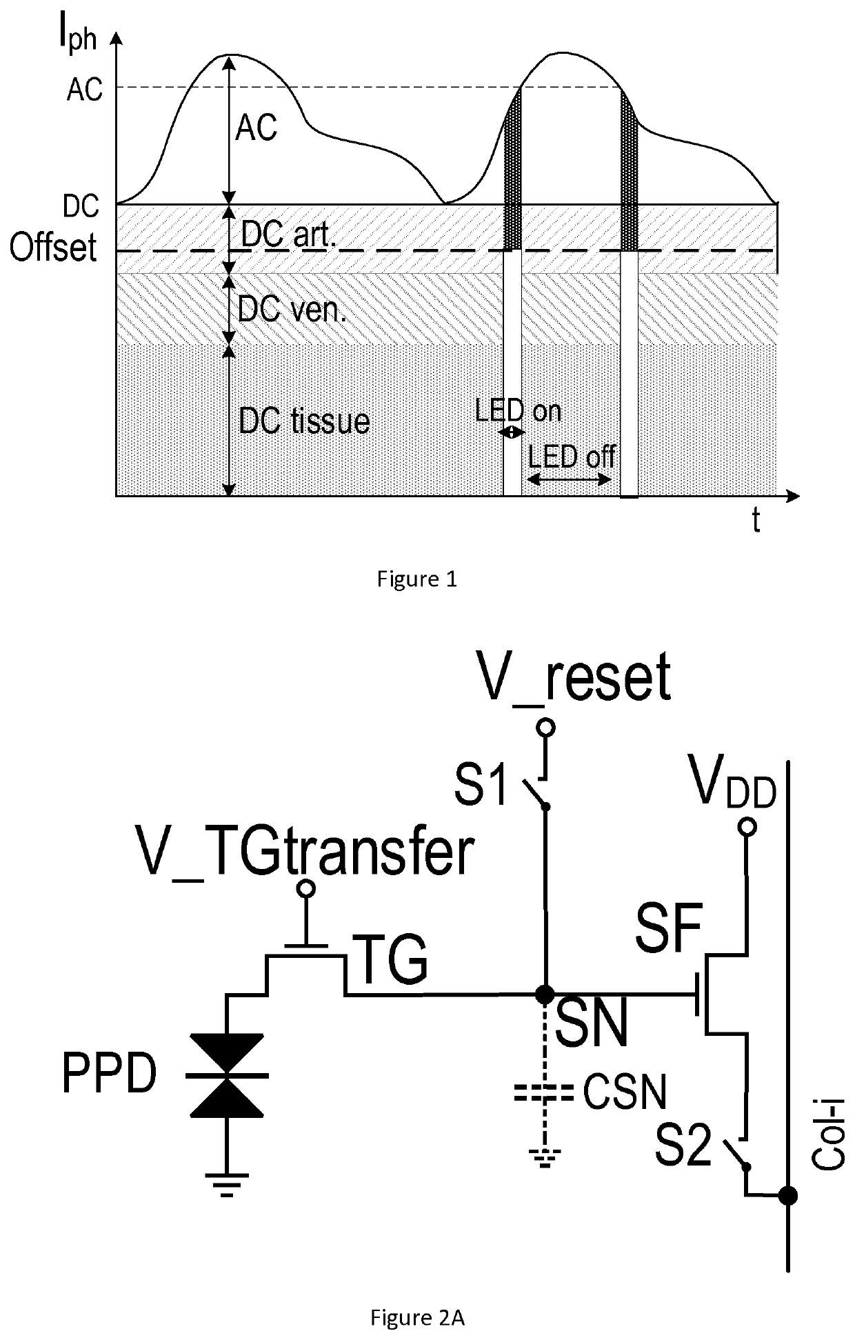
[0001]The present invention relates to the domain of CMOS sensors for biomedical applications, especially health monitoring.[0002]Nowadays, health monitoring is becoming increasingly important, given both the ageing of population and the combined action of an increase in obesity level and cardio-related pathologies, i.e. cardiovascular diseases. The healthcare industry is becoming more dependent on new methods to monitor patients.[0003]This, along with an increased interest in fitness and wellness, is calling for more affordable and precise health monitoring devices, especially when wearable.[0004]In such a context, photoplethysmography (PPG) is known and appears to be a key technology allowing non-invasive monitoring of vital biological indicators such as heart rate (HR), blood oxygen saturation (SpO2), respiration rate (RR), and arterial pressure (AP).[0005]A standard PPG system comprises pulsed LEDs synchronized with a photo-sensor and a processing chain. The LEDs diffuse light i...

Claims


Application Information

Patent Timeline
IPC IPC(8): A61B5/024
CPCA61B5/02427A61B5/7203A61B5/7246A61B5/0295A61B5/14552H01L27/14612A61B5/7225A61B2560/0247A61B2562/0233A61B2562/046A61B2562/12H04N25/46H04N25/50H04N25/77H01L27/14H04N25/00
Inventor BOUKHAYMA, ASSIMCAIZZONE, ANTONINOENZ, CHRISTIAN
Owner ECOLE POLYTECHNIQUE FEDERALE DE LAUSANNE (EPFL)
Learn More