Check patentability & draft patents in minutes with Patsnap Eureka AI!

Method and apparatus for designing resistive random access memory

a random access memory and resistive technology, applied in the field of semiconductor memory devices, can solve the problem that the overall performance of the resistive random access memory cannot be guaranteed, and achieve the effect of superior performan

Active Publication Date: 2020-08-13
INST OF MICROELECTRONICS CHINESE ACAD OF SCI
View PDF0 Cites 0 Cited by
  • Summary
  • Abstract
  • Description
  • Claims
  • Application Information

AI Technical Summary

Benefits of technology

This patent is about a method for selecting the materials used in a resistive random access memory device based on certain parameters. These parameters include the voltage needed to form the device, the voltage needed to set a memory cell, the time it takes to turn the device on and off, the power consumed, the time it takes to erase or write data to the device, the stability and durability of the device, and the on-off ratio of the device. By using this method, researchers can create more efficient and effective resistive random access memory devices by selecting the most suitable materials for each parameter.

Problems solved by technology

At present, when designing resistive random access memory, current experimental means and theoretical methods cannot fully consider the factors affecting the characteristics of resistive random access memory, resulting in that the overall performance of the resistive random access memory cannot be guaranteed.

Method used


Image

  • Method and apparatus for designing resistive random access memory
  • Method and apparatus for designing resistive random access memory

Examples


Embodiment Construction

[0036]Exemplary embodiments of the present disclosure will be described in more detail below with reference to the accompanying drawings. While the embodiments of the present application have been shown in the drawings, it should be appreciated that these embodiments are not limiting, and the invention can be implemented in other forms. These embodiments are provided only for the purpose of fully understanding the invention and conveying the scope of the invention to those skilled in the art.

[0037]The technical solution of the present disclosure will be further described in detail below with specific embodiments in combination with accompanying drawings.

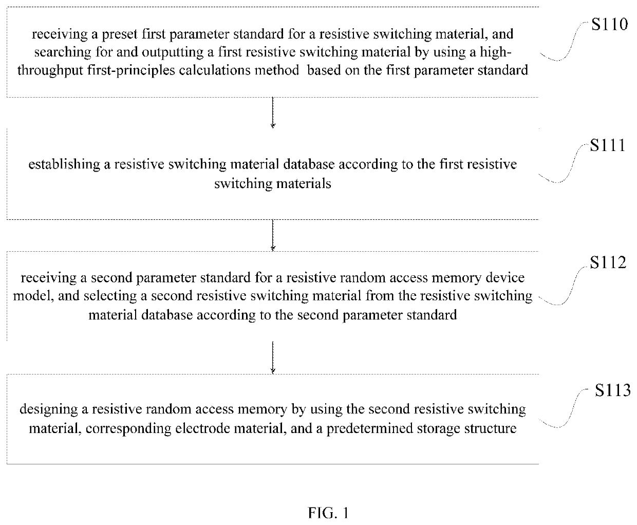
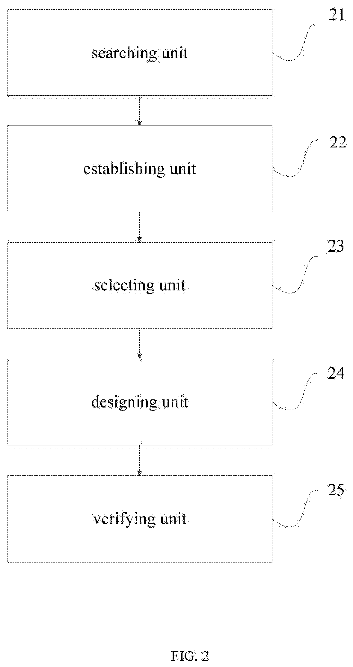
[0038]According to an embodiment of the disclosure, a method for designing a resistive random access memory is provided. As shown in FIG. 1, the method may comprise:

[0039]Step S110: receiving a preset first parameter standard for a resistive switching material, and searching for and outputting a first resistive switching material by ...


PUM

PropertyMeasurementUnit
band gapaaaaaaaaaa
band gapaaaaaaaaaa
band gapaaaaaaaaaa

Abstract

The disclosure provides a method and apparatus for designing a resistive random access memory, and the method comprise: receiving a preset first parameter standard of a resistive switching material, searching for and outputting a first resistive switching material based on the first parameter standard, first parameters including: band gap, charge transfer, vacancy, migration barrier, carrier activation energy. Schottky barrier and number of mesophase: establishing a resistive switching material database according to the first resistive switching materials; receiving a second parameter standard for a resistive random access memory device model, and selecting a second resistive switching material from the resistive switching material database according to the second parameter standard, second parameters including: Forming voltage, SET voltage, RESET voltage, erasing and writing speed, power consumption, storage window, stability, durability, on-off ratio, fluctuation of current parameter and storage density of the device model; and designing a resistive random access memory by using the second resistive switching material, corresponding electrode material, and a predetermined storage structure.

Description

TECHNICAL FIELD[0001]The present disclosure belongs to the technical field of semiconductor memory devices, and in particular, to a method and an apparatus for designing a resistive random access memory.BACKGROUND OF THE INVENTION[0002]With the rapid development of technologies such as big data, cloud computing, and Internet of Things, the data that need to be stored and processed in the world are increasingly growing, and better-performing memories are needed to meet the requirements of rapidly developing information technology for ultra-high-density storage.[0003]Resistive random access memories (RRAMs) have become popular to users due to their low operating power consumption, long durability, simple structure, and small device area. However, due to wide varieties of materials for resistive random access memory, the factors affecting the characteristics of resistive random access memory are diversified. At present, when designing resistive random access memory, current experimenta...

Claims


Application Information

Patent Timeline
Patent Type & Authority Applications(United States)
IPC IPC(8): G06F30/398G06F16/903
CPCG06F16/90335G06F30/398H01L45/08G06F2113/26H10B63/00H10N70/20H10N70/011H10B63/10G06F16/24569G06F30/39Y02D10/00H10N70/24
Inventor LU, NIANDUANLI, LINGLIU, MINGLIU, QI
Owner INST OF MICROELECTRONICS CHINESE ACAD OF SCI
Features
  • R&D
  • Intellectual Property
  • Life Sciences
  • Materials
  • Tech Scout
  • Unparalleled Data Quality
  • Higher Quality Content
  • 60% Fewer Hallucinations
Learn More