Press-in pin for an electrical contacting assembly

a technology of electrical contact and press-in pin, which is applied in the direction of soldering/welded conductive connections, line/current collector details, electrical apparatus, etc., can solve the problems of excessive deformation of copper layers, short circuits, and the mechanical system of the day press-in technology, and achieve low compressive stress and high load-bearing capacity.

Active Publication Date: 2020-10-29
ROBERT BOSCH GMBH
View PDF0 Cites 3 Cited by
  • Summary
  • Abstract
  • Description
  • Claims
  • Application Information

AI Technical Summary

Benefits of technology

[0007]The press-in pin for an electrical contact-making arrangement according to the invention has the advantage that connections with a high load-bearing capacity between the press-in pin and the metallized plated-through hole can be formed with very low compressive stresses and also tin-free surfaces. Embodiments of the press-in pin according to the invention can have any desired design with a reactive multilayer system as the surface and can be connected to the metallized plated-through hole in the printed circuit board by means of an appropriate joining method.
[0008]Embodiments of the invention describe a connection, which is based on an integrally joined connection, with a high mechanical load-bearing capacity between the press-in pin and the metallized plated-through hole on the basis of a novel tin-free coating of the press-in pin without any of the abovementioned disadvantages of the press-in pins known from the prior art, that is to say without forming tin whiskers and without mechanical damage due to excessive input of compressive stress into the printed circuit board or the metallized plated-through hole during the joining process.
[0011]Furthermore, the invention proposes a method for joining a press-in pin of this kind and a metallized plated-through hole which is inserted into a hole in a printed circuit board. The press-in pin is pushed into the metallized plated-through hole until a desired depth is reached. The reactive multilayer of the coating of the press-in pin is subsequently activated by an energy pulse which triggers an exothermic reaction of the reactive multilayer. Heat which is generated by the exothermic reaction melts the adjacent first contact layer of the press-in pin and the second contact layer of the metallized plated-through hole and welds said first contact layer and said second contact layer to one another to form an integrally joined connection. As a result, a connection with a high load-bearing capacity can be provided between the press-in pin and the metallized plated-through hole without high compressive stresses and without mechanical stress and without the risk of tin whiskers forming. Owing to the extremely short thermal input, there is advantageously no significant change in the microstructure of the metal. Owing to the subsequent exothermic reaction, the joining forces during “pressing in” of the press-in pin into the metallized plated-through hole can be considerably reduced. Therefore, it suffices to push the press-in pin only into the metallized plated-through hole. As a result, the compressive stresses in the metallized plated-through hole and in the printed circuit board can be reduced to a minimum required and all known faults of printed circuit board press-in technology can advantageously be avoided in a reliable manner. The greatly reduced joining forces provide a greater degree of freedom in terms of design when fitting the press-in pin to the leadframe. To this end, in addition to pressing the press-in pin into the metallized plated-through holes of the printed circuit board, a subsequent process for igniting the reactive multilayers has to be carried out.
[0012]It is particularly advantageous that the reactive multilayer is applied to an effective press-in length of the elastic press-in region. The reactive multilayer can be constructed, for example, from at least two different metal materials which are deposited alternately on the press-in pin in the correct phase with respect to each other. In this way, the press-in pin can be selectively coated with the reactive multilayer in the region of the effective press-in length. The two different metal materials can enter into a brief exothermic reaction in the event of appropriate activation. Since press-in pins are processed in very large numbers, the customary sputtering methods with deposition rates of between 2-6 μm / h described in the literature cannot be applied. Press-in pins are generally manufactured in stamped strips in a reel-to-reel manner and electrochemically coated by means of aqueous electrolytes in strip electroplating installations. This coating is usually performed selectively since the press-in pins very often require a different surface to the rest of the leadframe which often constitutes the contact pin or plug pin of a customer interface. Since not all metals can be deposited from aqueous electrolytes (for example aluminum) but reactive multilayer systems are often based on aluminum, the deposition of the reactive multilayer can be performed by means of special electrolytes from an aprotic solution, such as toluene for example, at elevated temperatures. To this end, a completely closed coating installation can preferably be used since the deposition takes place under an inert gas atmosphere.

Problems solved by technology

These tin whiskers can lead to short circuits.
A further disadvantage of present-day press-in technology is the mechanical system itself.
This creates typical press-in technology faults, such as excessive deformation of the copper layers, the jet effect, cracks in the sleeve and also the creation of electrically conductive particles (abrasion) for example.
Therefore, in summary, either high compressive stresses in the printed circuit board with a high probability of faults and / or tin-based pin surfaces with the risk of whisker formation are required for a connection with a high mechanical load-bearing capacity between the press-in pin and the plated-through hole.

Method used


Image

  • Press-in pin for an electrical contacting assembly
  • Press-in pin for an electrical contacting assembly
  • Press-in pin for an electrical contacting assembly

Examples


Embodiment Construction

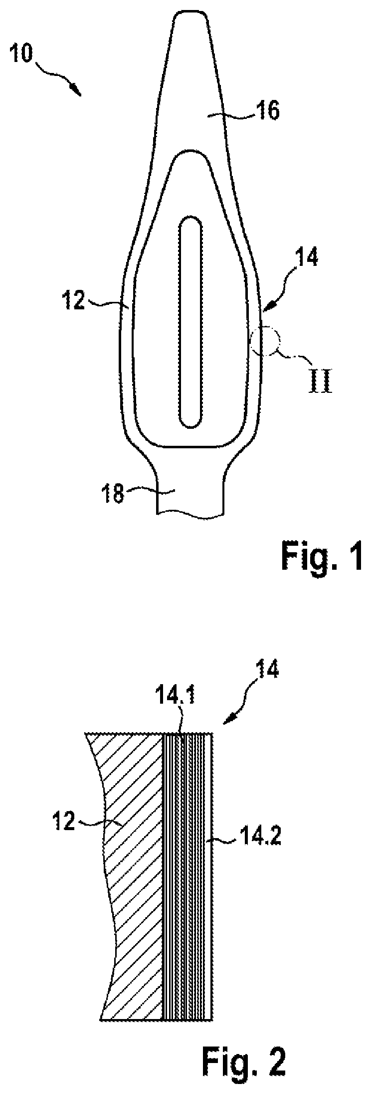
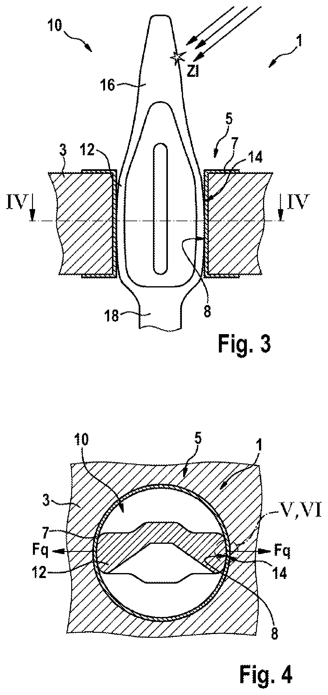
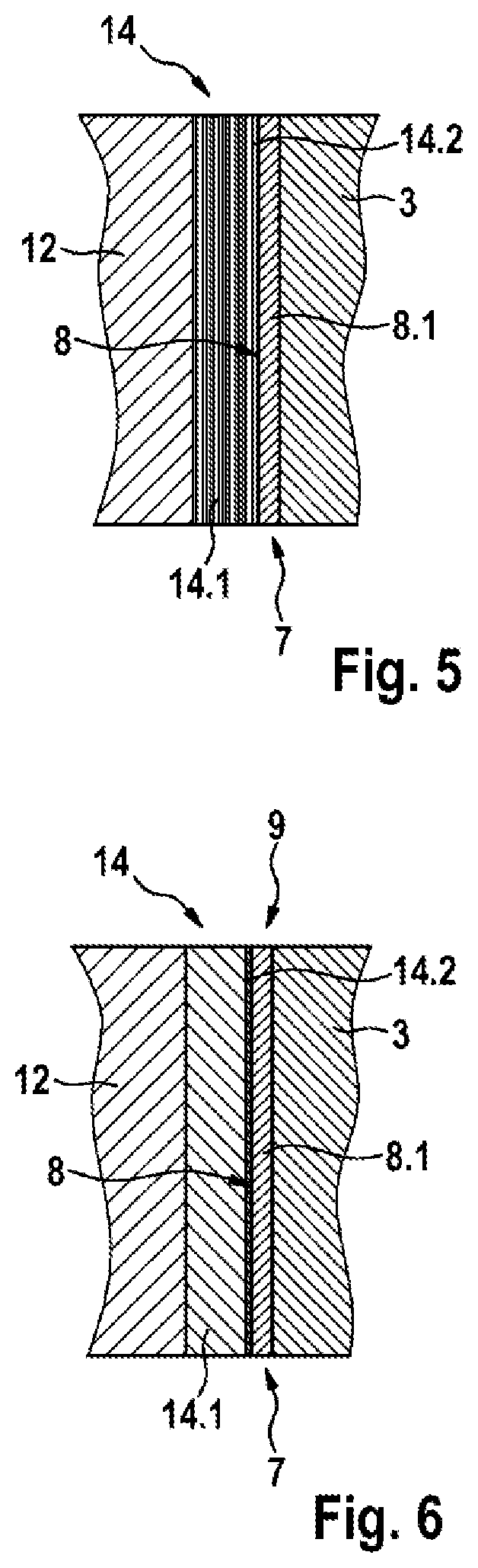
lass="d_n">[0023]As is shown in FIG. 1, the illustrated exemplary embodiment of a press-in pin 10 according to the invention for an electrical contact-making arrangement 1 comprises an elastic press-in region 12 and an electrically conductive coating 14. Here, the coating 14 comprises a reactive multilayer 14.1 which is applied to the press-in pin 10 and a first contact layer 14.2 which is applied to the reactive multilayer 14.1.

[0024]In the illustrated exemplary embodiment of the press-in pin 10, the reactive multilayer 14.1 is applied to an effective press-in length of the elastic press-in region 12. In the illustrated exemplary embodiment, the reactive multilayer 14.1 contains aluminum as the first metal material and nickel as the second metal material. The reactive multilayer 14.1, which is formed as a nickel-aluminum layer stack, has a releasing bond enthalpy of −59 kJ / mol and generates an adiabatic reaction temperature of 1639° C. It goes without saying that the reactive multi...


PUM

PropertyMeasurementUnit
deposition ratesaaaaaaaaaa
melting pointaaaaaaaaaa

Abstract

The invention relates to a press-in pin (10) for an electrical contacting assembly (1), having an elastic press-in region (12) and an electrically conductive coating (14). The invention further relates to a corresponding contacting assembly (1), and to a method for joining a press-in pin (10) and a metallized via (7). The coating (14) comprises a reactive multi-layer applied to the press-in pin (10) and a first contact layer applied to the reactive multi-layer.

Description

BACKGROUND OF THE INVENTION[0001]The invention proceeds from a press-in pin for an electrical contact-making arrangement comprising an elastic press-in region and an electrically conductive coating. The present invention also relates to an electrical contact-making arrangement comprising a press-in pin of this kind and also to a method for joining a press-in pin and a metallized plated-through hole.[0002]The prior art discloses printed circuit board press-in pins with a modest number of different coating variants. A distinction is made between tin-based coating variants and tin-free coating variants here. These different layer systems are used depending on the expected loading on the electromechanical connection between the press-in pin and the metallized plated-through hole. The mechanical connection between the press-in pin and the plated-through hole is based on a non-positively locking connection, a positively locking connection and an integrally joined connection. The non-posit...

Claims


Application Information

Patent Timeline
Patent Type & Authority Applications(United States)
IPC IPC(8): H01R12/58H01R4/02H01R43/02
CPCH01R12/585H01R4/025H01R43/0256H01R43/0221H05K3/308H05K3/325H05K2201/10303H05K2201/1059H05K2201/10878
Inventor LUDWIG, RONNYHACHTEL, ANDREASKLETT, GUSTAVSCHUERER, MARTIN
Owner ROBERT BOSCH GMBH
Why Eureka
Try Eureka