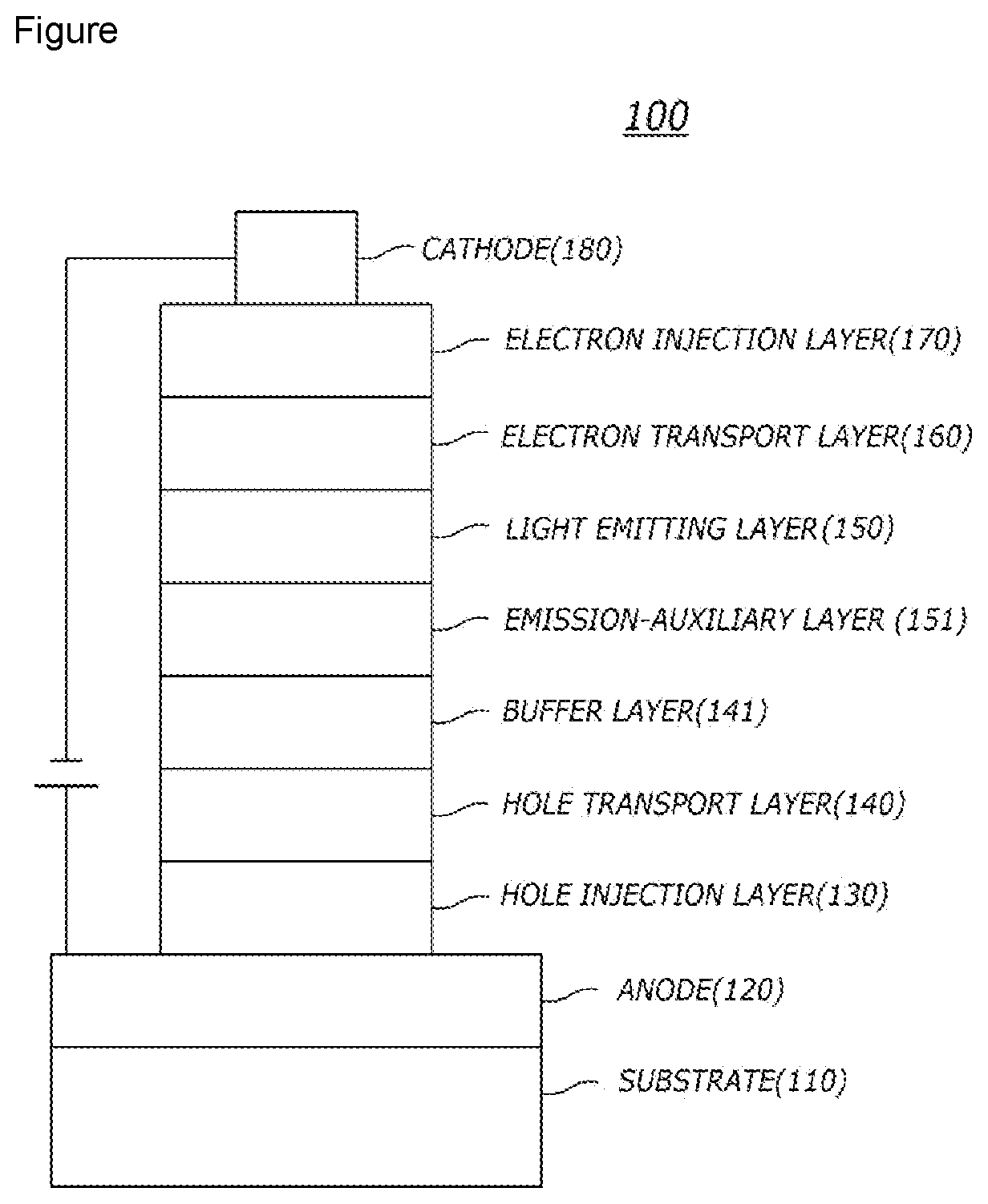
Compound for organic electroluminescent element, organic electroluminescent element using the same, and an electroluminescent device thereof
a technology of electroluminescent elements and organic electroluminescent elements, applied in the direction of luminescent compositions, organic chemistry, chemistry apparatus and processes, etc., can solve the problems of reducing the efficiency of a corresponding element, reducing the luminous efficiency, and shifting the maximum luminescence wavelength to a longer wavelength, so as to improve the luminous efficiency and lifetime, the driving voltage of the device can be lowered, and the effect of reducing the driving voltage of the elemen
- Summary
- Abstract
- Description
- Claims
- Application Information
AI Technical Summary
Benefits of technology
Problems solved by technology
Method used
Image

Examples
synthesis example
of Sub 2
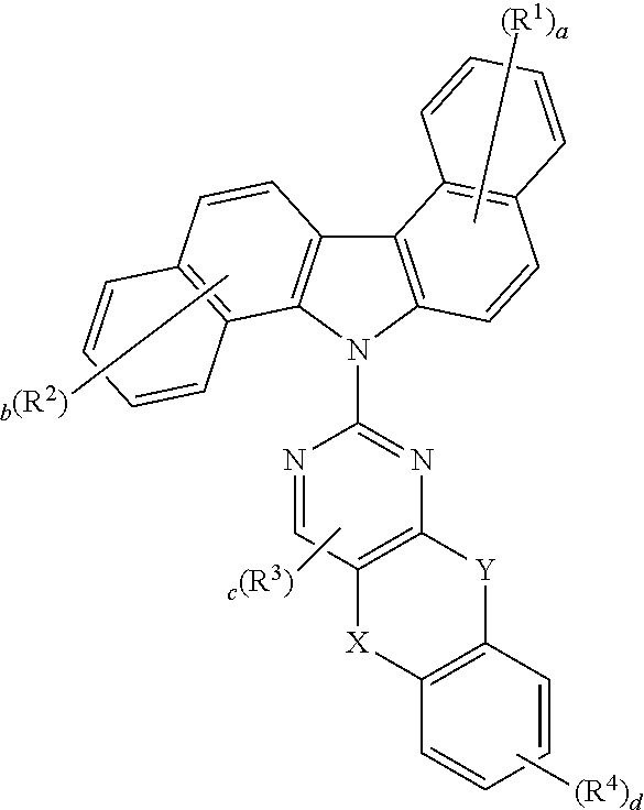
[0056]Sub 2 of the Reaction Scheme 1 may be synthesized by the reaction route of the following Reaction Scheme 3.
Synthesis of Sub 2(1a)
[0057]
[0058]Sub 2-1 (1) (5.1 g, 20 mmol), Sub 2-2 (1) (2.9 g, 24 mmol), Pd (PPh3)4 (0.7 g, 0.6 mmol), NaOH (2.4 g, 60 mmol), THF (60 mL), and water (30 mL) were placed into a round bottom flask and the mixture was heated at 80-90° C. under reflux. When the reaction was completed, the reaction product was diluted by adding distilled water at room temperature and the resultant was extracted with CH2Cl2 and water. The organic layer was dried with MgSO4 and concentrated. Thereafter, the concentrate was passed through a silica gel column and recrystallized to obtain 4.8 g of Sub 2(1a) (yield: 81%).
Synthesis of Sub 2(2a)
[0059]
[0060]Sub 2-1(2) (5.1 g, 20 mmol), Sub 2-2(1) (2.9 g, 24 mmol), Pd(PPh3)4 (0.7 g, 0.6 mmol), NaOH (2.4 g, 60 mmol), THF (60 mL) and water (30 mL) were placed into a round bottom flask and 5.0 g (yield: 85%) of Sub 2(2a) was ob...
example 1
[Example 1] Red OLED (Host)
[0075]After vacuum-depositing N1-(naphthalen-2-yl)-N4,N4-bis(4-(naphthalen-2-yl (phenyl)amino)phenyl)-N1-phenylbenzene-1,4-diamine (abbreviated as “2-TNATA”) film on an ITO layer(anode) to form a hole injection layer having a thickness of 60 nm, wherein the ITO layer was formed on a glass substrate, 4,4-bis[N-(1-naphthalenyl)-N-phenylamino (abbreviated as “NPD”) film was vacuum-deposited with a thickness of 60 nm on the hole injection layer to form a hole transport layer.
[0076]Next, the compound 1 of the present invention as a host material and bis-(1-phenylisoquinolyl)iridium(III)acetylacetonate (hereinafter “(piq)2Ir(acac)”) as a dopant material in a weight ratio of 95:5 were deposited on the hole transport layer to form a light emitting layer with a thickness of 30 nm.
[0077]Subsequently, (1,1′-biphenyl-4-olato)bis(2-methyl-8-quinolinolato)aluminum (abbreviated as “BAlq”) was vacuum-deposited with a thickness of 10 nm on the light emitting layer to form ...
example 18
[Example 2] to [Example 18]
[0079]The OLEDs were fabricated in the same manner as described in Example 1 except that the compounds of the present invention described in the following Table 3, instead of the compound 1 of the present invention, were used as host material of a light emitting layer.
PUM
| Property | Measurement | Unit |
|---|---|---|
| thickness | aaaaa | aaaaa |
| thickness | aaaaa | aaaaa |
| thickness | aaaaa | aaaaa |
Abstract
Description
Claims
Application Information
 - R&D
- Intellectual Property
- Life Sciences
- Materials
- Tech Scout
- Unparalleled Data Quality
- Higher Quality Content
- 60% Fewer Hallucinations
Browse by: Latest US Patents, China's latest patents, Technical Efficacy Thesaurus, Application Domain, Technology Topic, Popular Technical Reports.
© 2025 PatSnap. All rights reserved.Legal|Privacy policy|Modern Slavery Act Transparency Statement|Sitemap|About US| Contact US: help@patsnap.com