Flexible bootstrapping for power electronics circuits

a power electronics circuit and charging circuit technology, applied in pulse technique, process and machine control, instruments, etc., can solve the problems of high output voltage loss and distortion, shortening service life, overheating and catching fire, etc., and achieve the effect of preventing the discharging of the energy storage devi

Active Publication Date: 2020-12-17
DR ING H C F PORSCHE AG
View PDF0 Cites 8 Cited by
  • Summary
  • Abstract
  • Description
  • Claims
  • Application Information

AI Technical Summary

Benefits of technology

[0013]One aspect of this disclosure relates to a method for flexible bootstrapping in a power electronics circuit, in which an energy storage device used for controlling a power semiconductor switch and a source / emitter potential of the power semiconductor switch are at the same potential. A blocking diode is connected to a supply voltage that is provided by a source referenced to a reference potential, in such a way that the source can only emit, but not absorb, energy via said blocking diode. The blocking diode is followed by at least one bootstrap transistor, the drain / collector input of which is connected to the blocking diode and the source / emitter output to an upper potential of the energy storage device. At least one electrical component is designed to also pass a current flow in the blocking direction if a specified potential difference is exceeded. This component is connected with an input of the electrical component in the blocking direction to a gate / base control terminal of the bootstrap transistor and with an output of the electrical component to a terminal of the energy storage unit at the source / emitter potential of the power semiconductor switch, if the bootstrap transistor is an n-channel field effect transistor or an npn-bipolar transistor. The component is connected in the blocking direction with an input of the electrical component to an upper potential of the energy storage device and with an output of the electrical component to a gate / base control terminal of the bootstrap transistor if the bootstrap transistor is a p-channel field effect transistor or a pnp-bipolar transistor. Correspondingly, in the case of an n-channel field effect transistor or an npn-bipolar transistor as the bootstrap transistor, at least one resistor is arranged between a potential of the supply voltage and the gate / base control terminal of the bootstrap transistor and, in the case of a p-channel field effect transistor or a pnp-bipolar transistor as the bootstrap transistor, the resistor is arranged between the source / emitter potential of the power semiconductor switch and the gate / base control terminal of the bootstrap transistor. This causes a charging of the energy storage device as soon as the potential of the supply voltage is above a potential of the energy storage device, and prevents overcharging as soon as the potential difference specified in the electrical component is exceeded, and thereby preventing discharging of the energy storage device by the blocking diode. Additional resistors to the gate / base control input of the bootstrap transistor can be used to limit the current into or out of the gate / base control input of the bootstrap transistor.

Problems solved by technology

If a voltage required by a consumer deviates greatly from the battery voltage, a power electronics circuit causes high losses and distortions in the output voltage.
In particular, this has an adverse effect on a drive electric motor, which usually requires alternating voltages with significantly lower amplitude, particularly at low speeds, and also stresses its insulation, thereby shortening the service life.
A further problem with battery packs is that due to variation in the physical and chemical behaviors of the battery cells, in order to enable a uniform state of charge, a so-called battery management system must be provided, which includes an elaborate monitoring of the individual battery cells and, in particular, local charge exchange.
Furthermore, a fault in a single battery cell usually requires the entire battery pack to be shut down, as defective battery cells can overheat and catch fire under continued loading.
A problem with electronic semiconductor switches, especially with field effect transistors, abbreviated as FET, or with bipolar transistors with isolated gate electrodes, abbreviated as IGBT, is that they normally need to be controlled relative to their own potential.
However, such converters are expensive and inefficient.
However, in modular multilevel converters in particular, half-bridges with power semiconductor switches are also present in which for circuit design-related reasons a bootstrapping process cannot be used, since in some circuit configurations a bootstrap capacitor would become overloaded.
This problem can occur, for example, if the drain / collector terminals instead of the source / emitter terminals of the transistors to be switched are at the potential of the power supply, in particular if partitions of identical modules are formed within multilevel converters, in which transistors to be synchronously switched are conveniently combined into modules but as a result, some of the transistors can no longer be activated by conventional bootstrapping.
Furthermore, at these times the bootstrap capacitor would overload, since the current flow will not stop until the electrical potential of the positive pole of the bootstrap capacitor matches that of the positive terminal of the power supply.
This can be far too high.
Accordingly, without current limiting a sudden high current flow would occur, which can cause various problems including a collapse of the supply voltage, electromagnetic emissions, heating and / or damage to components and conductors.
To activate at a lower threshold and deactivate again only when an upper threshold is exceeded, such a threshold switch can be a Schmitt trigger and will therefore have hysteresis.

Method used


Image

  • Flexible bootstrapping for power electronics circuits
  • Flexible bootstrapping for power electronics circuits
  • Flexible bootstrapping for power electronics circuits

Examples


Embodiment Construction

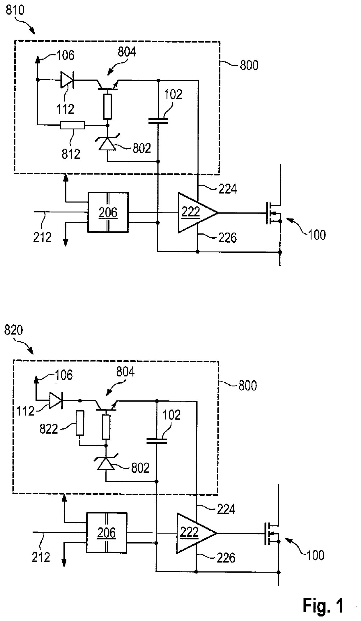
[0056]FIG. 1 shows a schematic representation of example circuits 810 and 820 for activating a power semiconductor switch using a bipolar transistor 804 by means of an embodiment of the method according to the invention. The bipolar transistor 804 fulfills the function of the charging switch, wherein its activation potential is different from the potential of the switching signal 212. Accordingly, a level shifter 206 can be optionally used for the control, which shifts the potential of the switching signal 212 to that of the source / emitter reference and which can be integrated together with the driver output stage of the gate driver 222. Preferably, the power is supplied on the input side of the level shifter 206 via the same potential as that of a controller that provides the switching signal 212. The use of an optocoupler or a signal isolator is also conceivable, wherein the switch used in this case does not need to be a power transistor, rather a small signal transistor may be su...


PUM

PropertyMeasurementUnit
threshold voltageaaaaaaaaaa
voltageaaaaaaaaaa
voltageaaaaaaaaaa

Abstract

The invention relates to a method and to a charging circuit (800) for flexible bootstrapping in power electronics circuits, comprising a blocking diode (112), at least one bootstrap transistor (804), at least one resistor (812, 822) and at least one electrical component (802), which is designed to conduct a current flow when a predetermined potential difference is exceeded. An energy storage device (102) used for controlling a power semiconductor switch (100) and a source/emitter potential of the power semiconductor switch (100) are at the same potential, charging of the energy storage device (102) being effected as soon as the potential of a supply voltage (106) is above a potential of the energy storage device (102). Overcharging is prevented as soon as the predetermined potential difference in the electrical component (802) is exceeded, and discharging of the energy storage device (102) is prevented by the blocking diode (112).

Description

BACKGROUNDField of the Invention[0001]The present invention relates to a method and a charging circuit for flexible bootstrapping in power electronics circuits, which are used, for example, in devices for providing an AC power supply from a battery pack. In addition, a multilevel converter that uses said method and charging circuit is claimed.Related Art[0002]Currently, battery packs usually installed in electric vehicles are hard-wired units, for example of individual battery cells. At the output, such batteries supply almost exclusively DC voltage, whereas most consumers in electric vehicles require an AC voltage with a certain frequency, amplitude and phase. In addition, the DC voltage supplied varies according to the state of charge. In order to be able to supply connected consumers with the required power both at a peak voltage and at a final charging voltage, up to now they have had to be equipped with elaborate supply circuits, e.g. with power semiconductor switches. If a vol...

Claims


Application Information

Patent Timeline
Patent Type & Authority Applications(United States)
IPC IPC(8): H02M1/088H02M3/155
CPCH02M1/088H02M3/155H02M2001/0048H03K19/0133H02M1/08H02M7/49H03K2217/0081H03K2217/0063H02M1/0006H02M7/4835Y02B70/10H02M1/0048
Inventor GOETZ, STEFAN
Owner DR ING H C F PORSCHE AG
Why Eureka
Try Eureka