Three-dimensional magnetic device and magnetic memory

Active Publication Date: 2021-01-07
XI AN JIAOTONG UNIV
View PDF0 Cites 1 Cited by
  • Summary
  • Abstract
  • Description
  • Claims
  • Application Information

AI Technical Summary

Benefits of technology

The present disclosure provides a three-dimensional magnetic device based on the spin Hall effect. By distributing the storage unit array on both the plane and vertical direction of the wafer substrate, the storage density can be improved multiple times while ensuring its thermal stability. The use of a spin-orbit torque to reverse magnetization and the separation of reading and writing operations can improve the reliability and stability of the device. The operation circuit promotes the practical application of the three-dimensional magnetic device. The magnetic junction structure and the use of a spin-orbit torque can increase the thermal stability factor. Overall, the present disclosure has wide industrial applicability.

Problems solved by technology

First, the critical writing current varies in inverse proportion to the writing time, and therefore a high-speed writing requires increasing the writing current, leading to high power consumption.
Second, the writing current needs to pass through the tunneling barrier of the MTJ, which is likely to be broken down.
Since the heavy metal layer and each layer of the MTJ are parallel to the wafer substrate surface, occupying large areas, it is difficult to miniaturize the MTJ array and realize a high storage density for the conventional two-dimensional MRAM.
74001, 2013), the scaling of a two-dimensional MTJ array has a limit, thus it is difficult to further improve the storage density of MRAM (A. Goyal et al., Appl. Phys. Lett., vol.

Method used


Image

  • Three-dimensional magnetic device and magnetic memory
  • Three-dimensional magnetic device and magnetic memory
  • Three-dimensional magnetic device and magnetic memory

Examples


Embodiment Construction

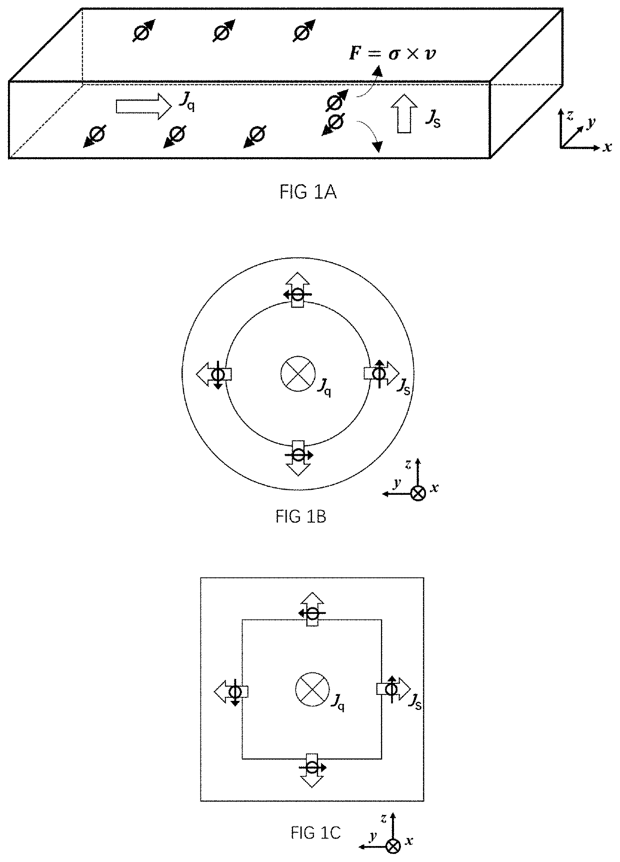
lass="d_n">[0048]FIG. 1A shows the spin Hall effect in a heavy metal material. When a charge current is introduced in the x direction, a spin-polarized current can be generated in the z direction.

[0049]FIG. 1B shows the spin Hall effect in a heavy metal material with a columnar structure and a circular cross section, which is coated with a layer of ferromagnetic material on the outer surface. When a charge current is introduced along the x direction into the heavy metal material, a spin-polarized current can be generated in the radial direction. The polarization of the spin-polarized current is oriented clockwise or counterclockwise along the tangent line. After spin-polarized electrons diffuse into the adjacent ferromagnetic layer, the electrons exchange spin angular momentum with the ferromagnetic layer, such that the magnetization of the ferromagnetic layer may be oriented clockwise or counterclockwise according to the selection.

[0050]FIG. 1C shows the spin Hall effect in a heavy...


PUM


Abstract

Disclosed is a three-dimensional magnetic device based on a spin Hall effect which includes an internal electrode, at least one magnetic junction and at least one external electrode. The internal electrode, the at least one magnetic junction and the at least one external electrode have columnar structures. Each of the at least one magnetic junction comprises a magnetic free layer, a magnetic reference layer and a non-magnetic spacing layer between magnetic free layer and magnetic reference layer. The magnetic free layer is in contact with internal electrode, and the magnetic reference layer in each of the at least one magnetic junction is in contact with a corresponding one of the at least one external electrode. The three-dimensional magnetic device may be stacked in a normal direction of the bottom surface of the internal electrode. Magnetization reversal of three-dimensional magnetic device may be realized by a combination of a spin-orbit torque and a spin transfer torque. The magnetic device has advantages of reduced heating, improved reliability and stability, high storage density while ensuring thermal stability.

Description

CROSS REFERENCE TO RELATED APPLICATION[0001]This application claims the priority of a Chinese patent application No. 201910600144.3 filed on Jul. 4, 2019, the disclosure of which is incorporated herein by reference in its entirety.BACKGROUNDField of the Disclosure[0002]The disclosure relates to devices and circuits and applications thereof having magnetic materials or structures, and in particular, to a three-dimensional magnetic device and its data writing mechanism based on spin Hall effect and a circuit thereof.Description of Related Art[0003]Magnetic random access memory (MRAM) has advantages of non-volatility, random access, low cost, high endurance (nearly unlimited reading and writing), wide operating temperature range and being radiation-harden (free from high-energy particle radiation interference).[0004]The core storage unit of MRAM is a magnetic tunnel junction (MTJ). The MTJ is essentially consisted of a reference layer, a spacing layer, and a free layer. The reference l...

Claims


Application Information

Patent Timeline
IPC IPC(8): G11C11/16G11C11/18H01L43/10H01L43/04
CPCG11C11/161G11C11/1675H01L43/04G11C11/18H01L43/10G11C11/1673G11C11/1659G11C11/155H10B61/20H10N50/85H10N50/01H10N50/10H10N52/80
Inventor MIN, TAIHAO, RUNZIWANG, LEIZHOU, XUE
Owner XI AN JIAOTONG UNIV
Why Eureka
Try Eureka