Fluidic Assembly Enabled Mass Transfer for MicroLED Displays

a technology of fluidic assembly and micro-leds, which is applied in the direction of semiconductor/solid-state device manufacturing, electrical equipment, semiconductor/semiconductor devices, etc., can solve the problems of image burn-in, limited contrast ratio, and less than 4% efficiency of lcd displays

Pending Publication Date: 2021-03-25
ELUX INC
View PDF0 Cites 10 Cited by
  • Summary
  • Abstract
  • Description
  • Claims
  • Application Information

AI Technical Summary

Benefits of technology

[0041]An associated microLED mass transfer method provides the fluidic assembly carrier substrate mentioned above, with an array of wells, and also provides the stamp substrate mentioned above, where each trap site in the array is configured with a columnar-shaped recess having the same pitch as the carrier substrate wells. The method uses a fluidic assembly process to fill the carrier substrate wells with microLEDs. The method presses the stamp substrate top surface against the carrier substrate top surface, with each trap site interfacing a corresponding well, and transfers the microLEDs from the carrier substrate to the stamp substrate. Each trap site recess confines a keel extending from a microLED bottom surface, and in response to confining each microLED keel, the microLEDs are secured to the stamp substrate. The use of the carrier substrate eliminates the limitations imposed by the pitch of the microLEDs on the MOCVD wafer, thus permitting the use of a variety of stamp substrate pitches for different display substrate sizes and resolutions.

Problems solved by technology

As a consequence, the efficiency of an LCD display may be less than 4% and the contrast ratio is limited by light leaking through the cell.
OLED pixels are direct emitting so the display contrast ratio is high, but the organic materials can be subject to long term degradation causing image burn-in.
Because each microLED is handled separately the assembly process is painfully slow.
Increasing the indium content moves the emission peak to longer wavelengths, but also increases the stress due to lattice mismatch, so high-efficiency GaN devices cannot be made for red emission, and the efficiency of green emitting devices is lower than that of blue LEDs.
Because the microLEDs are quite small, more of the area of the MOCVD wafer is removed in the patterning process, decreasing the available emission area from each wafer.
LED wafers are relatively expensive and the high-resolution processing for microLED fabrication further increases cost, so it is very important to use the emission area as efficiently as possible to minimize the cost of materials for a microLED display.
Because GaAs is opaque, the laser lift off technique cannot be used to remove GaAs based LEDs from the growth substrate.
The pick-and-place assembly presented here has several important weaknesses that lead to high cost and lower yield.
The assembly process is inherently serial, so assembling millions of microLEDs takes a long time and is expensive.
The very small size of the microLED makes construction of a pickup head quite difficult, and it is possible that the edges of the mechanism can interfere with adjacent microLEDs in pickup or the reflector structure on assembly.
However, the mass transfer methods can have poor yield because of defective microLEDs in the group being transferred, and because the pitch of the microLEDs is determined by the spacing of devices on the growth wafer.
This mass transfer assembly method is feasible and displays have been made this way, but there are several significant weaknesses that cause poor yield and high costs.
It is possible to customize the spacing of microLEDs on the MOCVD growth wafer for each display size and resolution, but this increases the cost of each microLED unreasonably.
Second, the pickup mechanism must strike a balance between too much and too little connection strength.
If the attachment is too weak some microLEDs are not captured from the carrier substrate, leaving a gap in the array.
In both cases the subpixel will be dark, which cannot be tolerated in a display.
Finally, the transfer stamp can be complex and difficult to fabricate.
This can be difficult for the complex holding methods that require the generation of a local field like electrostatic or magnetic attraction.
a) Missing microLED because of poor adhesion to the stamp at pickup;
b) Misplaced microLED from contamination on stamp;c) Particle caused by contamination of the transfer stamp;d) Broken microLED;e) Shorted microLED caused by a defect in the MOCVD process;f) MicroLED pulled out by the stamp causing electrode damage.
Another limitation of the simple mass transfer process described above is imposed by the square shape of the stamp, which is incommensurate with the circular wafers used for the MOCVD growth of LEDs. FIG. 4A shows a possible arrangement of 14×14 mm stamp capture regions on a 100 mm wafer, which might be a typical arrangement.
Larger stamp area increases assembly speed at the cost of leaving behind more microLEDs on the growth wafer.
The requirement that all of the stamp be filled leaves relatively large areas of a wafer which cannot be accessed.
The mechanical contact can disrupt insulating surface oxides, which improves wetting of the solder material.

Method used


Image

  • Fluidic Assembly Enabled Mass Transfer for MicroLED Displays
  • Fluidic Assembly Enabled Mass Transfer for MicroLED Displays
  • Fluidic Assembly Enabled Mass Transfer for MicroLED Displays

Examples


Embodiment Construction

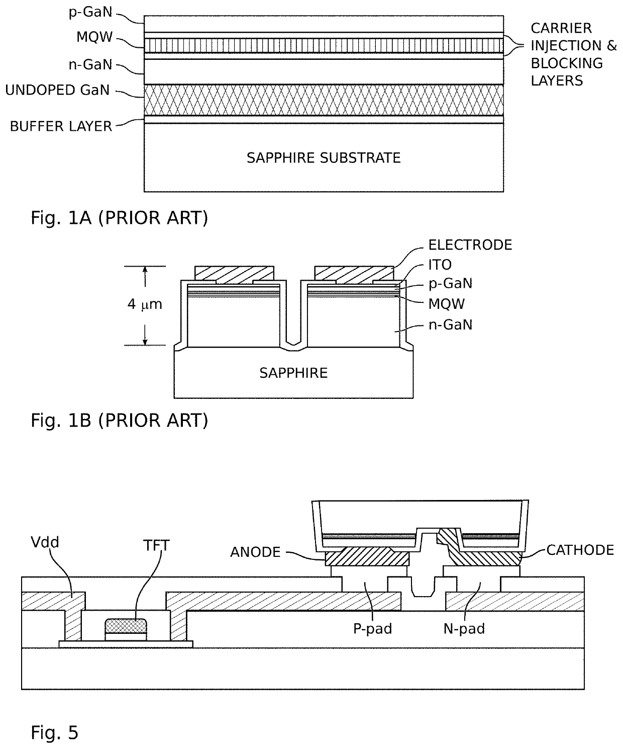
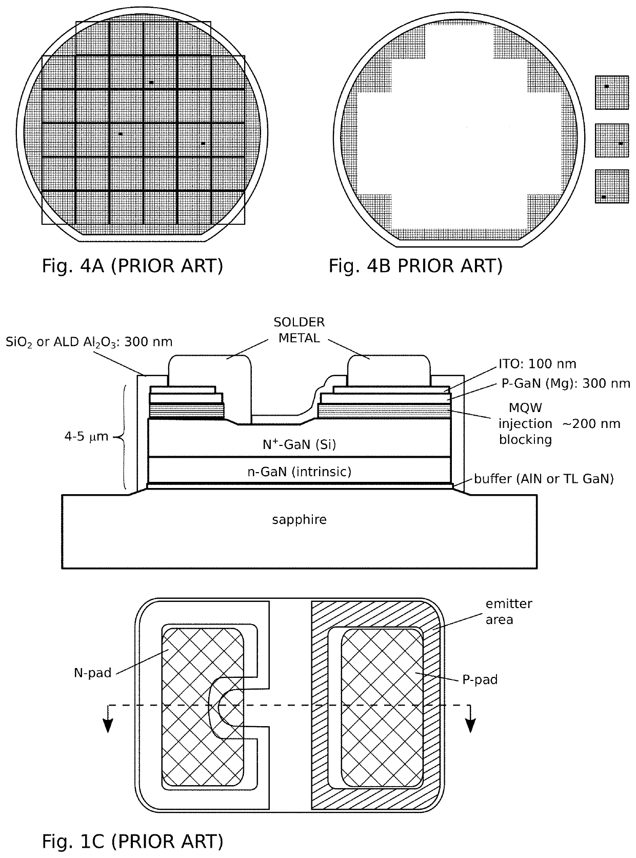
[0066]The general process for making a microLED display using inorganic LEDs and fluidic assembly on a display backplane has been reported in U.S. Pat. Nos. 9,825,202 and 10,418,527, which are incorporated herein by reference. In particular, the process flow for making a suitable display backplane is described in U.S. Pat. No. 9,825,202 starting at Col. 13 ln. 26, and shown in FIG. 17. The electrical requirements are described in pending application Ser. No. 16 / 727,186, which is also incorporated herein by reference. The display substrate used herein has the same row and column arrangement and thin-film transistor (TFT) circuits as previously described in U.S. Pat. No. 9,825,202 in FIGS. 14B and 14C, but there is no well layer because the mass transfer stamp sets the location of the microLED.

[0067]FIG. 5 is a partial cross-sectional view of an exemplary backplane arrangement showing one surface mount microLED and the power transistor which controls the brightness of the microLED.

[00...


PUM

PropertyMeasurementUnit
diameteraaaaaaaaaa
thicknessaaaaaaaaaa
diameteraaaaaaaaaa

Abstract

A microLED mass transfer stamping system includes a stamp substrate with an array of trap sites, each configured with a columnar-shaped recess to temporarily secure a keel extended from a bottom surface of a microLED. In the case of surface mount microLEDs, the keel is electrically nonconductive. In the case of vertical microLEDs, the keel is an electrically conductive second electrode. The stamping system also includes a fluidic assembly carrier substrate with an array of wells having a pitch separating adjacent wells that matches the pitch separating the stamp substrate trap sites. A display substrate includes an array of microLED pads with the same pitch as the trap sites. The stamp substrate top surface is pressed against the display substrate, with each trap site interfacing a corresponding microLED site, and the microLEDs are transferred. Fluidic assembly stamp substrates are also presented for use with microLEDs having keels or axial leads.

Description

RELATED APPLICATIONS[0001]Any and all applications, if any, for which a foreign or domestic priority claim is identified in the Application Data Sheet of the present application are hereby incorporated by reference under 37 CFR 1.57.BACKGROUND OF THE INVENTION1. Field of the Invention[0002]This invention generally relates to micro-light emitting diode (micro-LED) displays and, more particularly, to systems and methods for the mass transfer of microLEDs in the process of display fabrication.2. Description of the Related Art[0003]A red-green-blue (RGB) display is composed of pixels that emit light at three wavelengths corresponding to the visible colors red, green, and blue. The RGB components of the pixel, each of which is referred to as a sub-pixel, are energized in a systematic way to additively produce the colors of the visible spectrum. There are several display types that produce the RGB images in different ways. Liquid crystal displays (LCDs) are the most prevalent technology a...

Claims


Application Information

Patent Timeline
Patent Type & Authority Applications(United States)
IPC IPC(8): H01L25/075H01L33/48H01L33/38
CPCH01L25/0753H01L33/486H01L2933/0033H01L2933/0066H01L33/38H01L21/7806H01L33/0095H01L25/167H01L21/67144H01L24/19H01L24/20H01L2924/12041H01L24/95H01L2924/10155H01L2224/06102H01L2224/83851H01L2224/29111H01L2224/29144H01L2224/75705H01L2224/95085H01L21/6835H01L2224/7598H01L25/50H01L2224/83203H01L2224/83815H01L2224/83447H01L2224/8348H01L2224/95H01L2224/95101H01L2924/181H01L2224/04105H01L2224/73267H01L2224/92244H01L2224/83001H01L2224/73103H01L24/73H01L24/81H01L24/83H01L24/92H01L2224/9211H01L24/32H01L2224/32227H01L2224/16227H01L2224/32237H01L2224/16237H01L2224/32058H01L2224/75702H01L24/75H01L2224/83005H01L2224/81005H01L2224/75745H01L2224/75725H01L2224/75735H01L24/16H01L24/29H01L2224/13144H01L2224/13147H01L24/13H01L2224/11462H01L2221/68322H01L2221/68354H01L2221/68363H01L2924/014H01L2924/01049H01L2924/00014H01L2924/01032H01L2224/83H01L2924/00012H01L2224/81H01L21/67316H01L21/67343H01L21/70
Inventor SCHUELE, PAUL J.SASAKI, KENJIULMER, KURTLEE, JONG-JAN
Owner ELUX INC
Why Eureka
Try Eureka