Organic electric element comprising compound for organic electric element and electronic device thereof
a technology of organic electric elements and compound, which is applied in the direction of organic chemistry, luminescent compositions, chemistry apparatus and processes, etc., can solve the problems of inability to maximize efficiency and require more power consumption, and achieve the effects of increasing heat resistance, reducing driving voltage, and increasing luminous efficiency
- Summary
- Abstract
- Description
- Claims
- Application Information
AI Technical Summary
Benefits of technology
Problems solved by technology
Method used
Image
Examples
synthesis example
[0085]The following final products were synthesized with reference to the synthetic method disclosed in Korean Patent Registration No. 10-1530049 filed by the present applicant (registration-published on Jun. 18, 2015), Korean Patent Publication No. 10-2017-0112865 (published on Oct. 12, 2017), Korean Patent Publication No. 10-2017-0112913 (published on Oct. 12, 2017).
[0086]Synthesis of 1-19′
[0087]After putting N-([1,1′-biphenyl]-4-yl)naphthalen-1-amine (10 g, 33.6 mmol), 2-bromodibenzo[b,d]thiophene (9.8 g, 37.2 mmol), Pd2(dba)3 (1.55 g, 1.7 mmol), P(t-Bu)3 (0.68 g, 3.38 mmol), NaOt-Bu (10.76 g, 112 mmol) and toluene (355 mL) into a round bottom flask, the reaction was carried out at 100° C. When the reaction was completed, the reaction product was extracted with CH2Cl2 and water. The organic layer was dried with MgSO4 and concentrated. The concentrate was passed through a silica gel column and recrystallized to obtain 12.3 g (yield: 76%) of the product.
[0088]Synthesis of 1-20′
[008...
example 1
[Example 1] Red OLED (Host)
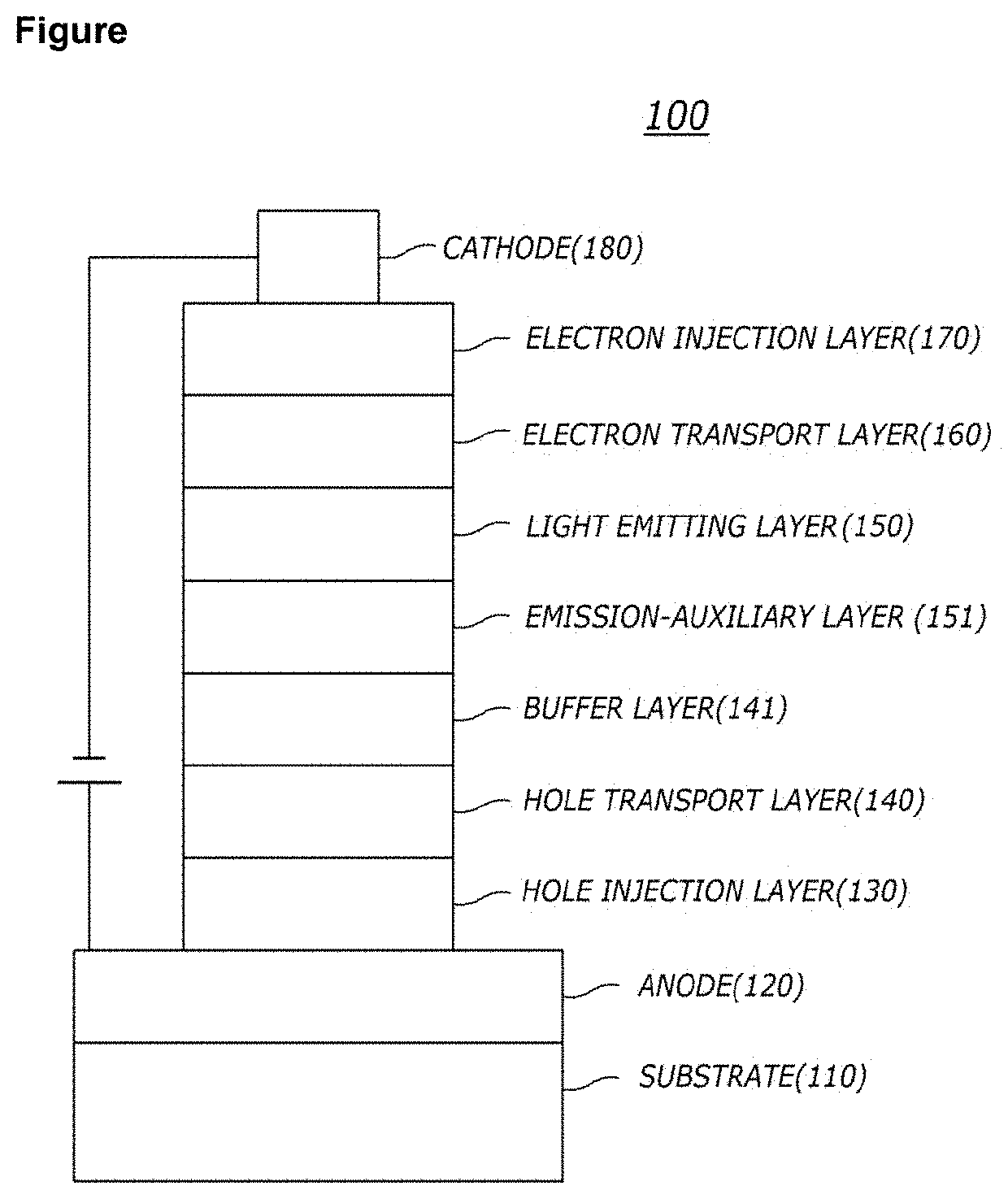
[0127]After vacuum-depositing N1-(naphthalen-2-yl)-N4,N4-bis(4-(naphthalen-2-yl(phenyl)amino)phenyl)-N1-phenylbenzene-1,4-diamine (hereinafter, “2-TNATA”) on an ITO layer (anode) formed on a glass substrate to form a hole injection layer with a thickness of 60 nm, a hole transport layer with a thickness of 60 nm was formed by vacuum-depositing the compound 1-33′ of the present invention on the hole injection layer.
[0128]Thereafter, on the hole transport layer, the compound 1-26′ of the present invention was vacuum-deposited to a thickness of 20 nm to form an emission-auxiliary layer.
[0129]Next, on the emission-auxiliary layer, the compound 3-5 of the present invention as a host material and bis-(1-phenylisoquinolyl)iridium(III)acetylacetonate (hereinafter, “(piq)2Ir(acac)”) as a dopant material in a weight ratio of 95:5 were deposited on the hole transport layer to form a light emitting layer with a thickness of 30 nm.
[0130]Next, 1,1′-bisphenyl-4-olato)bis...
example 2 to example 207
[0132]An organic electroluminescent element was manufactured in the same manner as in Example 1, using the compounds shown in Table 1 below as a material for the hole transport layer, the emission-auxiliary layer and the light emitting layer.
PUM
| Property | Measurement | Unit |
|---|---|---|
| temperature | aaaaa | aaaaa |
| thickness | aaaaa | aaaaa |
| thickness | aaaaa | aaaaa |
Abstract
Description
Claims
Application Information


