

Manufacturing method for semiconductor device
- Summary
- Abstract
- Description
- Claims
- Application Information
AI Technical Summary
Benefits of technology
Problems solved by technology
Method used
Image

Examples
Embodiment Construction
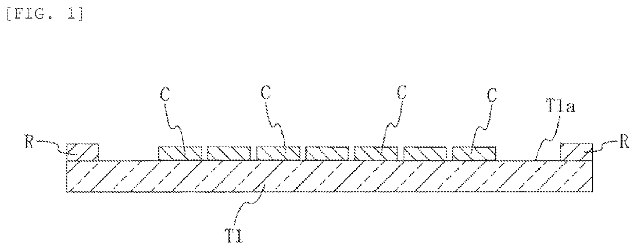
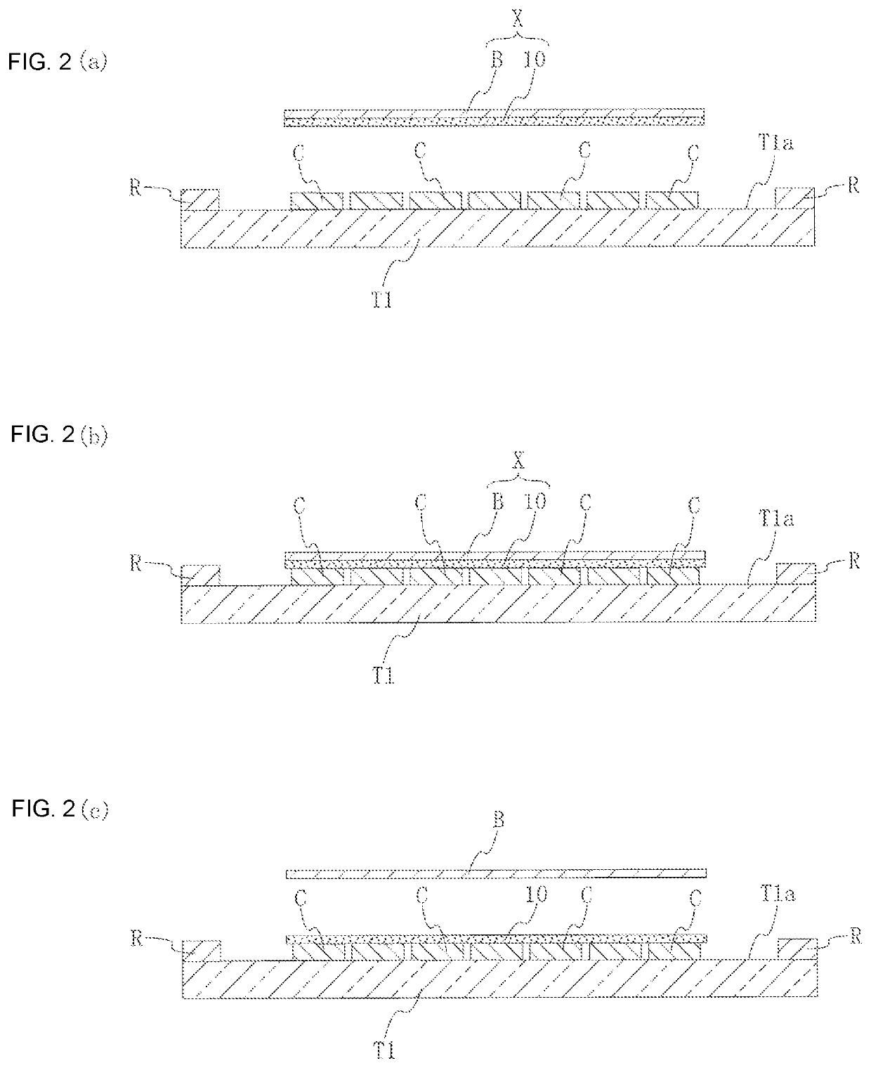
[0036]FIGS. 1 to 6 illustrate a semiconductor device manufacturing method according to one embodiment of the present invention. The semiconductor device manufacturing method according to the embodiment is a method for manufacturing a power semiconductor device or another semiconductor device including semiconductor chips in sinter-bonded areas and includes an arrangement step, a transfer step, a picking-up step, a temporary securing step, and a sinter bonding step as follows.
[0037]In the arrangement step, chips C are arranged on a processing tape T1, as illustrated in FIG. 1. The processing tape T1 typically has a multilayer structure including a carrier (base) and a pressure-sensitive adhesive layer and has, on one side, an adhesive face T1a defined by the pressure-sensitive adhesive layer. To the periphery of the adhesive face T1a of the processing tape T1, a ring frame R adheres. The ring frame R is a member with which a conveying mechanism, such as a conveying arm, is in mechani...
PUM
 Abstract
Description
Claims
Application Information