

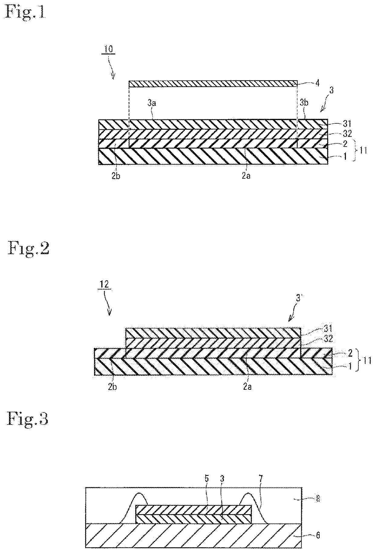
Sheet for heat bonding and sheet for heat bonding having dicing tape
a technology of heat bonding and dicing tape, which is applied in the direction of film/foil adhesives, solid-state devices, synthetic resin layered products, etc., can solve the problems of high heat dissipation properties and low electric resistivity of electrically conductive adhesives used in power semiconductor devices, and the heat characteristics and reliability of solder and electrically conductive adhesives
- Summary
- Abstract
- Description
- Claims
- Application Information
AI Technical Summary
Benefits of technology
Problems solved by technology
Method used
Image

Examples
example 1
[0173]
[0174]A solution (12 wt %) prepared by previously dissolving a thermally decomposable binder A in MEK at a weight ratio of 1:1, a low boiling point binder A (4 wt %), metal fine particles A (60 wt %), and an organic solvent A (24% by weight) were placed in a stirring pot of a hybrid mixer (HM-500, manufactured by Keyence Corporation), and stirred and mixed in a stirring mode for 3 minutes.
[0175]The varnish thus obtained was applied to a release-treated film (MRA 38 manufactured by Mitsubishi Plastics Co., Ltd.) so as to have a thickness after drying of 70 μm, and dried to obtain a pre-sintering layer A. The drying was performed at 80° C. for 2 minutes.
[0176]
[0177]A solution (50 wt %) obtained by previously dissolving a thermally decomposable binder A in MEK at a weight ratio of 1:1 and an organic solvent A (50 wt %) were placed in a stirring pot of a hybrid mixer (HM-500 manufactured by Keyence Corporation), and stirred and mixed in a stirring mode for 3 minutes.
[0178]The obta...
example 2
[0181]
[0182]The varnish for the component migration prevention layer A of Example 1 was used, applied so as to have a thickness after drying of 6 μm, and dried to obtain a component migration prevention layer B.
[0183]
[0184]The coating dried surfaces of the pre-sintering layer A and component migration prevention layer B were made to face each other, and laminated to each other at 70° C. with a hydraulic laminator to obtain a sheet for heat bonding B.
[0185][Evaluation of Component Migration Suppression]
[0186]
[0187]100 parts of 2-ethylhexyl acrylate, 19 parts of 2-hydroxyethyl acrylate, 0.4 parts of benzoyl peroxide, and 80 parts of toluene were placed in a reaction vessel equipped with a condenser, a nitrogen inlet tube, a thermometer, and a stirring device, and polymerized at 60° C. for 10 hours in a nitrogen stream to obtain an acrylic polymer A.
[0188]1.2 parts of 2-methacryloyloxyethyl isocyanate was added to the acrylic polymer A to obtain a mixture, and the mixture was subjected...
PUM
| Property | Measurement | Unit |
|---|---|---|
| thickness | aaaaa | aaaaa |
| thickness | aaaaa | aaaaa |
| temperature | aaaaa | aaaaa |
Abstract
Description
Claims
Application Information