Method for preparing optical metasurfaces

a technology of optical metasurfaces and optical metasurfaces, applied in the field of micronano processing, can solve the problems of limiting the practical application of optics, the limited industrialization of metasurface-based optical elements, and the high cost of electron beam lithography machines, so as to improve the production cost and production time, reduce costs, and reduce production costs

Inactive Publication Date: 2021-07-15
SOUTH UNIVERSITY OF SCIENCE AND TECHNOLOGY OF CHINA
View PDF0 Cites 5 Cited by
  • Summary
  • Abstract
  • Description
  • Claims
  • Application Information

AI Technical Summary

Benefits of technology

[0047]The method for preparing optical metasurfaces provided by the present application can replace the electron beam lithography method used in fabricating meta-atoms, greatly reducing the costs, and greatly reducing the production time. The method provided by the present application is suitable for industrial production. When the same pattern of meta-atoms is subjected to a large number of repetitive inscriptions, the electron beam lithography method needs to inscribe the pattern one by one, and the electron beam lithography needs to be used for a long time. However, the electron beam lithography is used for only one time to fabricate the nickel template in the method provided by the present appli

Problems solved by technology

However, the challenges encountered in nano-processing of three-dimensional metamaterials and their huge optical losses limit its practical application in the field of optics.
Limited by the small beam of the electron beam and the electron beam photoresist requires a certain amount of exposure to effectively transfe

Method used


Image

  • Method for preparing optical metasurfaces
  • Method for preparing optical metasurfaces
  • Method for preparing optical metasurfaces

Examples


example 2

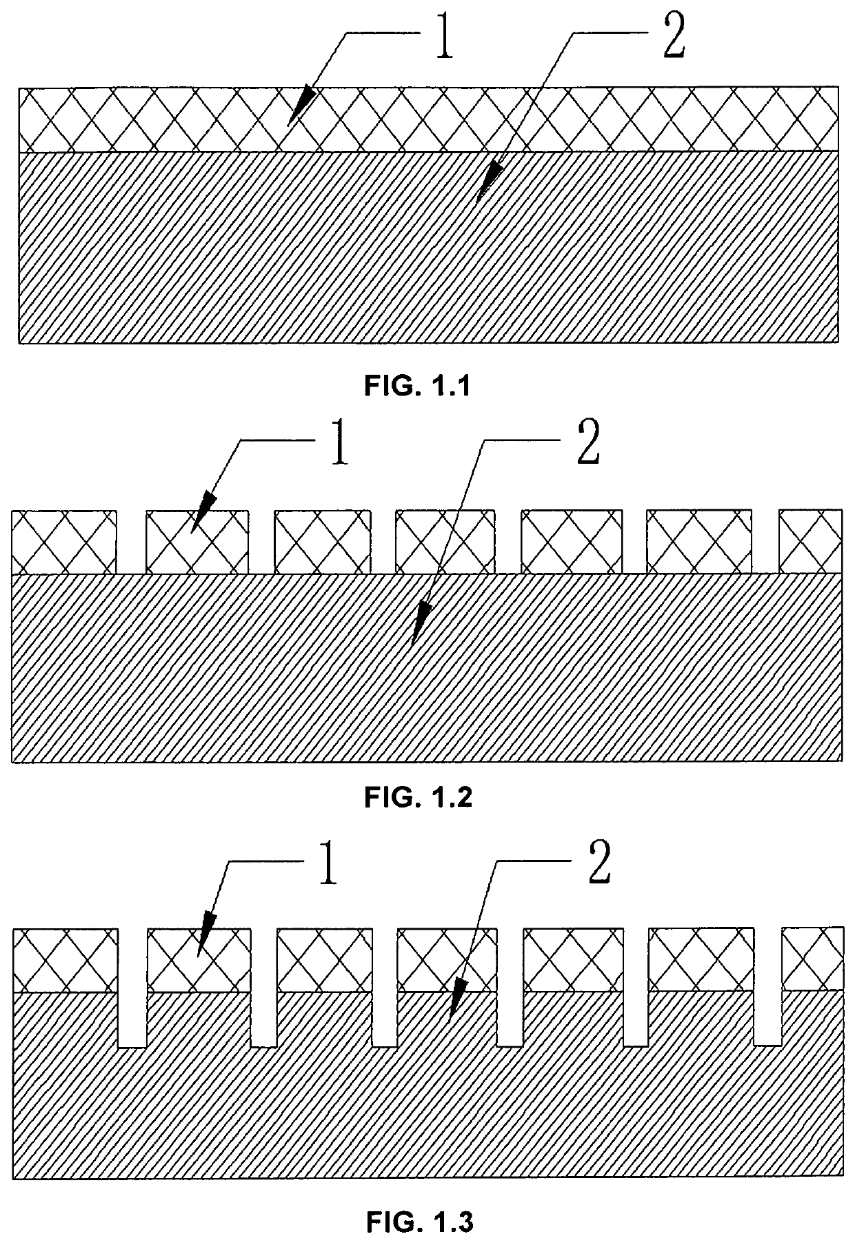
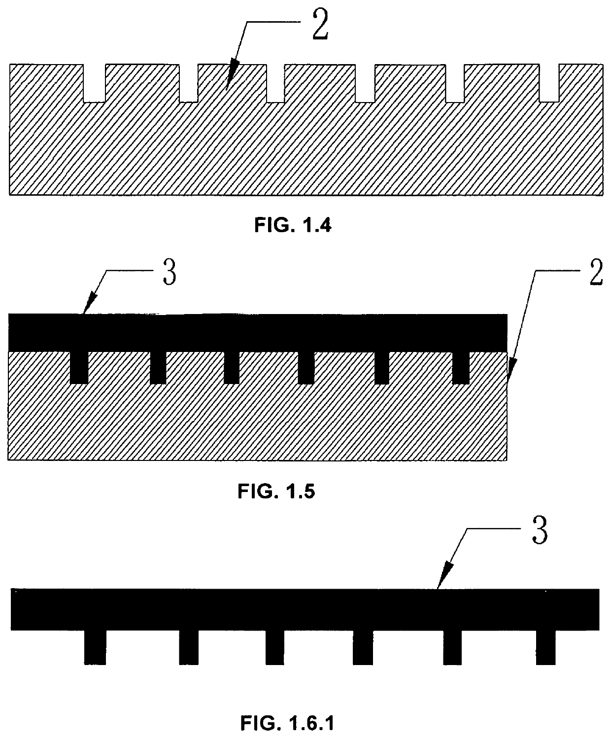
[0086]This example provides a method for preparing an optical metasurface-based optical element, which was performed based on nano-imprinting. The specific method is as follows:[0087]a. A silicon wafer with designed patterns of metasurface-atoms 9 was prepared referring to the four steps a, b, c, and d of Example 1 (a schematic view of the product shown in FIG. 2.1).[0088]b. the patterns on the silicon wafer with designed patterns of metasurface-atoms 9 were transferred onto a polymer film 10 (such as PC, PMMA, PEEK, PI, PET, PU, PTFE, PVDF, or PDMS, etc.) by using a nano-imprinting method (a schematic view of the product shown in FIG. 2.2);[0089]c. the polymer film 10 was separated from the silicon wafer 9, and the patterns on the silicon wafer 9 were transferred onto the polymer film 10 to complete the fabrication of a nano-imprinting template (a schematic view of the product shown in FIG. 2.3);[0090]d. a metal reflective layer constituting the metasurface-based optical element 6 ...

example 3

[0093]This example provides a method for preparing an optical metasurface-based optical element, which was performed based on nano-imprinting. The specific method is as follows:[0094]a. a nano-imprinting resist having good adhesion with transparent substrate 12 was spin-coated on a transparent substrate 13. The nano-imprinting resist 12 was imprinted with the fabricated Ni metal imprinting template or polymer film imprinting template 11 with designed patterns of metasurface-atoms to transfer the patterns onto the nano-imprinting resist 12 (a schematic view of the product shown in FIG. 3.1). Specific process for transferring and process for cleaning after transferring were referred to steps h and i of Example 1;[0095]b. the nano-imprinting resist 12 was used as a mask to etch the transparent substrate 13. The depth for etching was the thickness of the designed metal layer of the metasurface-atoms (a schematic view of the product shown in FIG. 3.2);[0096]c. a metal layer constituting ...


PUM


Abstract

The present application discloses a method for preparing optical metasurfaces, wherein the method is performed based on nano-imprinting, and the template used in the method is an imprinting template with patterns of meta-atoms. The method for preparing optical metasurfaces provided by the present application can replace the electron beam lithography method used in fabricating meta-atoms, greatly reducing the costs, and greatly reducing the production time. The method provided by the present application significantly improves the production cost and the production time, achieving a low-cost, large-scale fabrication of metasurface-based optical elements within a short time, and having good industrialization prospects.

Description

TECHNICAL FIELD[0001]The present application relates to the field of micro-nano processing, in particular, relates to the preparation of optical metasurfaces.BACKGROUND[0002]Optical metamaterials are optical structural materials designed and constructed artificially in which the meta-atoms allow light to propagate in a way that is impossible for natural materials. The linear optical parameters of the metamaterials, such as effective dielectric constant, magnetic permeability, refractive index, etc., can be designed by regulating the constituent materials and geometry of the meta-atoms. In this way, the electromagnetic response of the meta-atoms is no longer limited to its own chemical composition. Some unique optical physical phenomena, such as negative refraction, super-resolution imaging and optical stealth etc., can be achieved through a rational design of optical metamaterials. However, the challenges encountered in nano-processing of three-dimensional metamaterials and their hu...

Claims


Application Information

Patent Timeline
IPC IPC(8): G03F1/78G03F7/033G03F1/60
CPCG03F1/78G03F1/60G03F7/033G03F7/0002G03F7/2037G03F7/40G03F7/0005B82Y40/00B82Y20/00G02B1/002
Inventor CHENG, XINGLI, GUIXINZHUANG, XINDENG, JUNHONG
Owner SOUTH UNIVERSITY OF SCIENCE AND TECHNOLOGY OF CHINA
Why Eureka
Try Eureka