
Dispersing Element, Method for Manufacturing Structure with Conductive Pattern Using the Same, and Structure with Conductive Pattern

Active Publication Date: 2021-07-22
ASAHI KASEI KOGYO KK
View PDF0 Cites 0 Cited by
  • Summary
  • Abstract
  • Description
  • Claims
  • Application Information

AI Technical Summary

Benefits of technology

The present invention allows for the creation of a conductive pattern that is highly stable and has low resistance on a circuit board. Additionally, the conductive pattern can be used for screen-printing and is stable over time in its resistivity. The pattern is also excellent in soldering performance.

Problems solved by technology

However, the conventional method has drawbacks, such as a large number of steps, complicated processing, and the necessity of a photoresist material.
For example, since the number of steps is small and the use of the photoresist material is unnecessary, this technique features significantly high productivity.
However, the copper in the form of ultrafine particles of several tens of nanometers is likely to oxidize and therefore an antioxidant treatment is required.
The antioxidant treatment had a problem of hindering sintering.

Method used


Image

  • Dispersing Element, Method for Manufacturing Structure with Conductive Pattern Using the Same, and Structure with Conductive Pattern
  • Dispersing Element, Method for Manufacturing Structure with Conductive Pattern Using the Same, and Structure with Conductive Pattern
  • Dispersing Element, Method for Manufacturing Structure with Conductive Pattern Using the Same, and Structure with Conductive Pattern

Examples


first embodiment

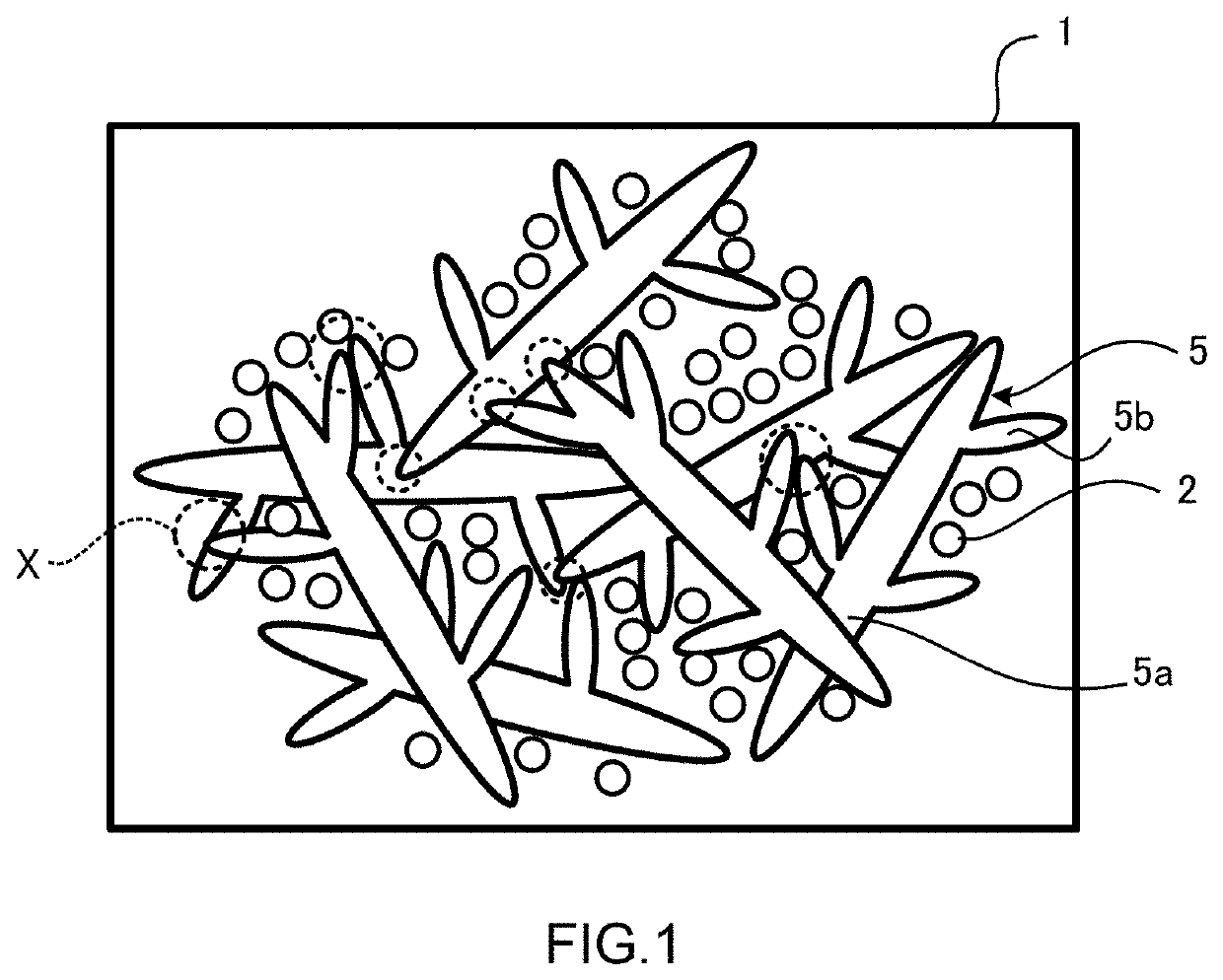
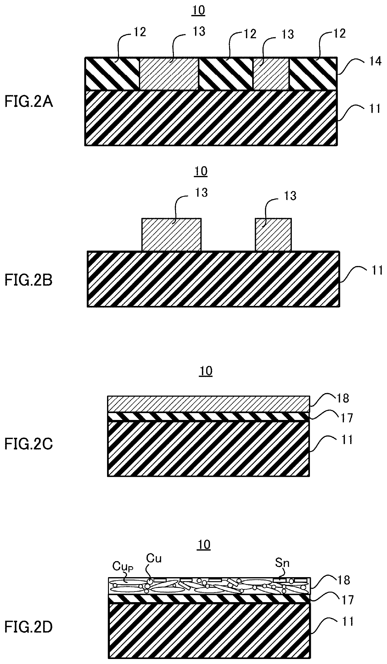
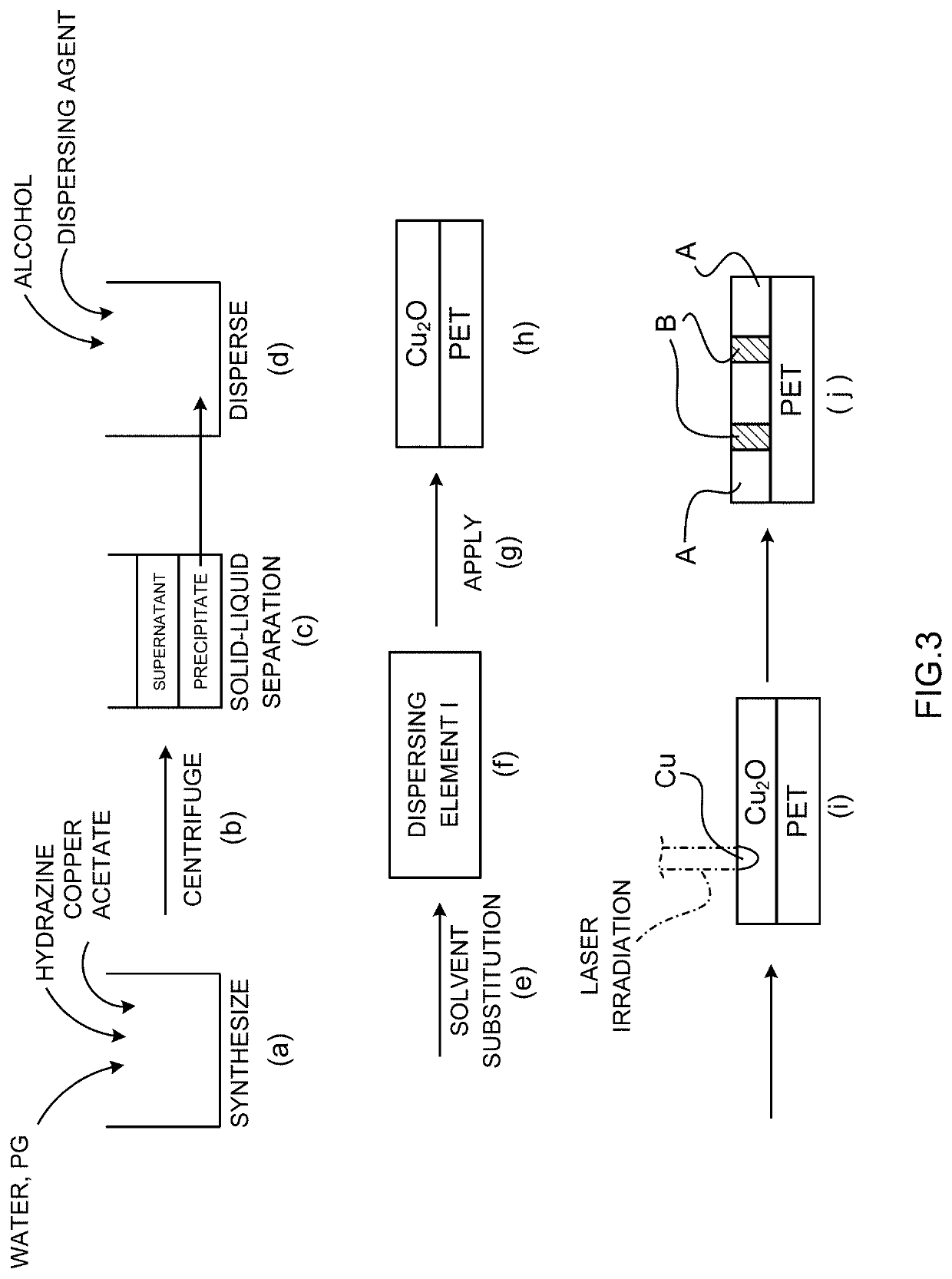
[0072]A dispersing element of the first embodiment contains (1) copper oxide, (2) dispersing agent, and (3) reductant. The dispersing element containing the reductant promotes reduction of copper oxide to copper in firing and promotes sintering of the copper.

[0073]The content of the reductant meets a range of the following formula (1). A mass ratio of the reductant of 0.0001 or more improves dispersion stability and decreases a resistance of a copper film. Additionally, the mass ratio of 0.1 or less improves long-term stability of the dispersing element.

0.0001≤(reductant mass / copper oxide mass)≤0.10  (1)

[0074]The content of the dispersing agent meets a range of the following formula (2). This reduces aggregation of the copper oxide and improves the dispersion stability.

0.0050≤(dispersing agent mass / copper oxide mass)≤0.30  (2)

[0075]The dispersing element of the first embodiment is limited in the ranges of the masses of the reductant and the dispersing agent to that of the copper oxi...

second embodiment

[0080]As a result of diligent examination, the inventors have found the following. The use of the copper oxide particles having specific particle diameters and the copper particles having specific particle diameters in combination for the dispersing element and the use of the dispersing agent reduce both cracks generated in sintering and cracks generated over time, thereby ensuring obtaining a conductive film having low resistivity and excellent stability of resistivity over time.

[0081]It has been found that although the above-described dispersing element contains the ultrafine particles in high concentration, the dispersing element is less likely to aggregate. Accordingly, it has been found that the dispersing element is also applicable to the screen-printing method and is excellent in printability. Moreover, it has been found that the above-described dispersing element exhibits excellent dispersion stability against a change over time in high concentration and allows screen-printi...

third embodiment

[0102]As a result of diligent examination, the inventors have found the following. The use of the dispersing element containing the copper oxide particles and the copper particles having a specific grain shape can obtain a conductive film that reduces both cracks generated during sintering and cracks generated over time, and has low resistivity and excellent stability of resistivity over time.

[0103]It has been found that although the above-described dispersing element contains the ultrafine particles in high concentration, the dispersing element is less likely to aggregate. Accordingly, it has been found that the dispersing element is also applicable to the screen-printing method and is excellent in printability. Moreover, it has been found that the above-described dispersing element exhibits excellent dispersion stability against a change over time in high concentration and allows screen-printing even after storage over a long period of time.

[0104]Furthermore, it has been found tha...


PUM


Abstract

A conductive pattern having high dispersion stability and a low resistance over a board is formed. A dispersing element (1) contains a copper oxide (2), a dispersing agent (3), and a reductant. Content of the reductant is in a range of a following formula (1). Content of the dispersing agent is in a range of a following formula (2).0.0001≤(reductant mass / copper oxide mass)≤0.10  (1)0.0050≤(dispersing agent mass / copper oxide mass)≤0.30  (2)The dispersing element containing the reductant promotes reduction of copper oxide to copper in firing and promotes sintering of the copper.

Description

TECHNICAL FIELD[0001]The present invention relates to a dispersing element, a method for manufacturing a structure with a conductive pattern using the same, and the structure with the conductive pattern.BACKGROUND ART[0002]A circuit board has a structure where conductive wiring is wired on a board. A method for manufacturing the circuit board is typically as follows. First, a photoresist is applied over a board with a stuck metal foil. Next, the photoresist is exposed and developed to obtain a negative appearance of a desired circuit pattern. Next, a part of the metal foil not coated with the photoresist is removed by chemical etching to form a pattern. Thus, high-performance circuit boards can be manufactured.[0003]However, the conventional method has drawbacks, such as a large number of steps, complicated processing, and the necessity of a photoresist material.[0004]In contrast to this, a direct wiring printing technique (hereinafter referred to as printed electronics (PE) method)...

Claims


Application Information

Patent Timeline
IPC IPC(8): H01B1/22H01B13/008H05K1/09H05K3/12
CPCH01B1/22H01B13/008H05K2203/0117H05K3/1291H05K1/092C09D11/52H01B13/0026H01B13/003H05K1/097H05K3/105H05K3/125H05K2201/0245H05K2203/1131H05K2203/1157H01B1/026H05K3/12H05K1/09
Inventor OHNO, EIICHIYUMOTO, TORUTSURUTA, MASANORI
Owner ASAHI KASEI KOGYO KK
Learn More