Copper/ceramic bonded body, insulating circuit substrate, copper/ceramic bonded body production method, and insulating circuit substrate production method

Pending Publication Date: 2021-08-05
MITSUBISHI MATERIALS CORP
View PDF0 Cites 0 Cited by
  • Summary
  • Abstract
  • Description
  • Claims
  • Application Information

AI Technical Summary

Benefits of technology

[0043]According to the present invention, it becomes possible to provide a copper/ceramic bonded body in which a copper member and a ceramic member are reliably bonded to each other, excellent migration resistance is achieved, and th

Problems solved by technology

For example, a power semiconductor element for large power control, which is used to control wind power gener

Method used


Image

  • Copper/ceramic bonded body, insulating circuit substrate, copper/ceramic bonded body production method, and insulating circuit substrate production method
  • Copper/ceramic bonded body, insulating circuit substrate, copper/ceramic bonded body production method, and insulating circuit substrate production method
  • Copper/ceramic bonded body, insulating circuit substrate, copper/ceramic bonded body production method, and insulating circuit substrate production method

Examples


examples 1 to 12

, Comparative Examples 1 to 2, Related Art Example

[0110]A confirmatory experiment performed to confirm the effectiveness of the present invention will be described.

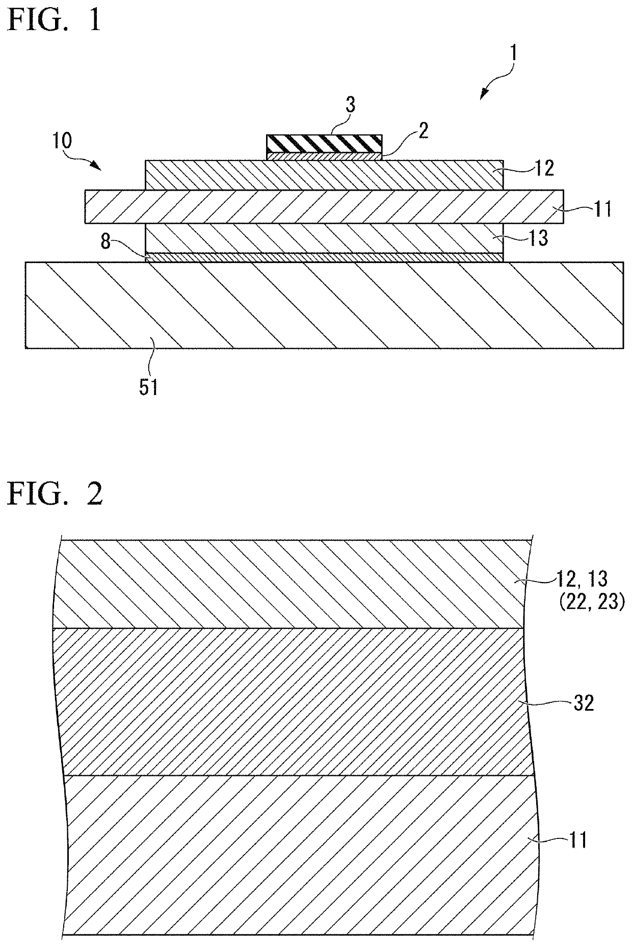
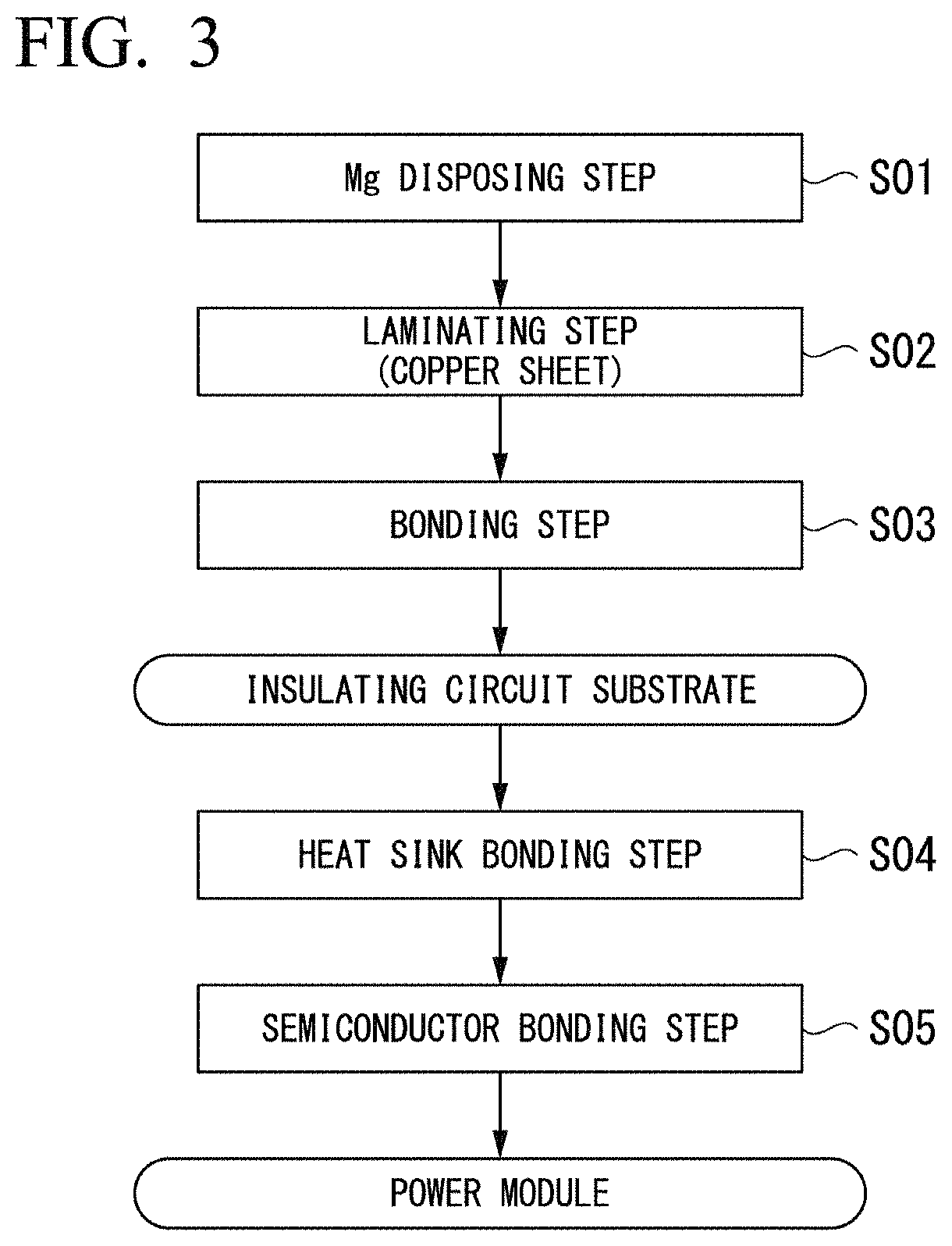
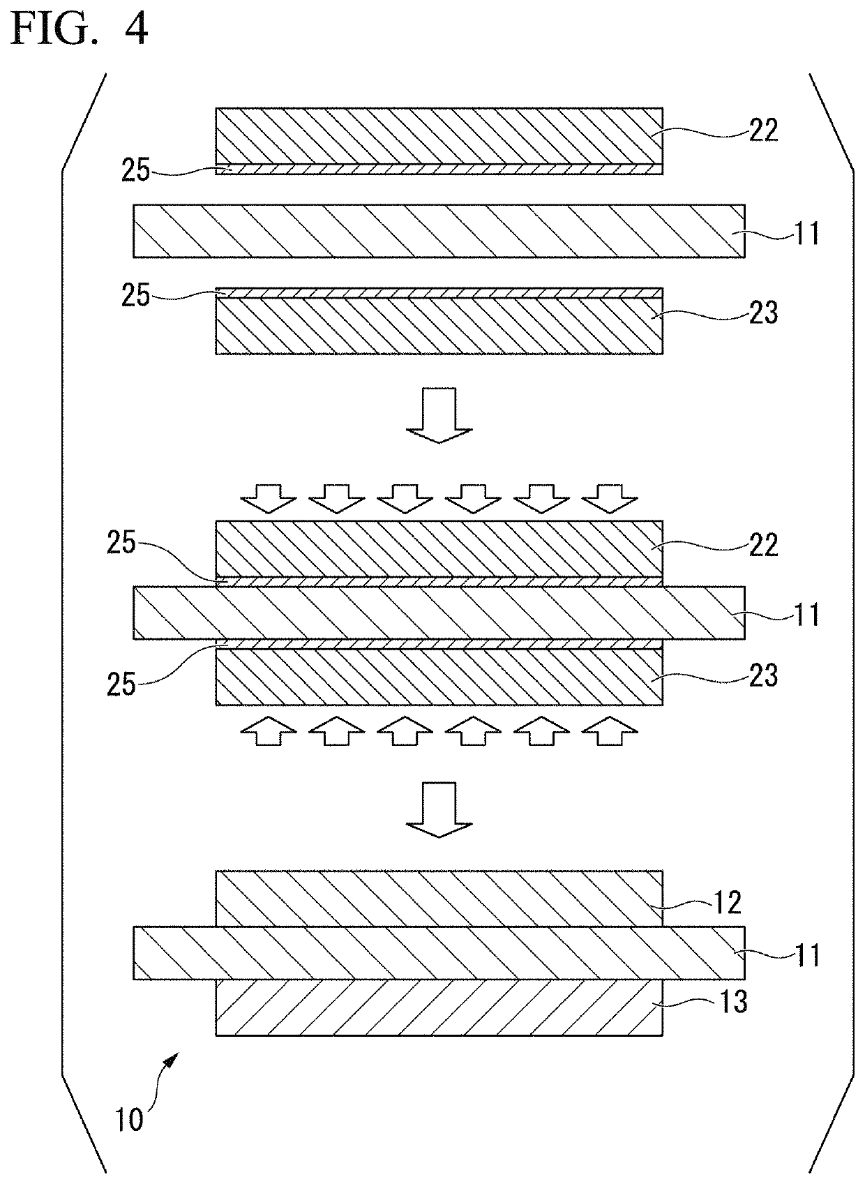
[0111]A copper / ceramic bonded body was formed by laminating copper sheets (oxygen-free copper, 37 mm square, thickness 0.15 mm) in which Mg was disposed as shown in Table 1, on both surfaces of a 40 mm square ceramic substrate made of an aluminum nitride and bonding the laminated sheets under bonding conditions shown in Table 1. The thickness of the ceramic substrate was 0.635 mm. In addition, the degree of vacuum of the vacuum furnace at the time of bonding was 5×10⁻³ Pa.

[0112]In a related art example, an active brazing material of Ag-28 mass % Cu-5 mass % Ti was disposed between the ceramic substrate and the copper sheet so that the amount of Ag was 5.2 mg / cm2.

[0113]In addition, when the temperature in the bonding step S03 was lowered from the bonding temperature (“Temperature (° C.)” in Table 1) to 480° C., the tempera...

examples 21 to 32

[0133]Copper / ceramic bonded bodies were produced in the same manner as the copper / ceramic bonded bodies produced in Examples 1 to 12, and regarding the obtained copper / ceramic bonded bodies, the area ratio of Cu2Mg and an ultrasonic bonded interface were evaluated as follows.

[0134]The evaluations of the area ratios of the Mg solid solution layer and the Cu—Mg intermetallic compound phase, and the initial bonding rate of the copper / ceramic bonded body were performed in the same manner as in the evaluations performed in Examples 1 to 12.

[0135](Temperature-Lowering Rate)

[0136]In the bonding step S03, when the temperature was lowered from the bonding temperature (“Temperature (° C.)” in Table 2) to 480° C., the temperature-lowering rate was controlled to be the rate shown in Table 2.

[0137](Area Ratio of Cu2Mg)

[0138]In the Cu—Mg intermetallic compound phase, the area ratio (%) of Cu2Mg was defined and calculated by the following calculation formula.

Area ratio (%) of Cu2Mg=area of Cu2Mg / (...


PUM

PropertyMeasurementUnit
Temperatureaaaaaaaaaa
Lengthaaaaaaaaaa

Abstract

A copper/ceramic bonded body includes: a copper member made of copper or a copper alloy; and a ceramic member made of an aluminum nitride, wherein, the copper member and the ceramic member are bonded to each other, and a Mg solid solution layer is provided between the copper member and the ceramic member and contains Mg in a state of a solid solution in a Cu primary phase.

Description

TECHNICAL FIELD[0001]This invention relates to a copper / ceramic bonded body in which a copper member made of copper or a copper alloy and a ceramic member made of an aluminum nitride are bonded to each other, an insulating circuit substrate, a copper / ceramic bonded body production method, and an insulating circuit substrate production method.[0002]Priority is claimed on Japanese Patent Application No. 2018-159457, filed Aug. 28, 2018, the content of which is incorporated herein by reference.BACKGROUND ART[0003]A power module, an LED module, and a thermoelectric module have a structure in which a power semiconductor element, an LED element, or a thermoelectric element is bonded to an insulating circuit substrate in which a circuit layer made of a conductive material is formed on one surface of an insulating layer.[0004]For example, a power semiconductor element for large power control, which is used to control wind power generation, an electric vehicle, a hybrid vehicle, and the like...

Claims


Application Information

Patent Timeline
IPC IPC(8): C04B37/02C04B35/581
CPCC04B37/023H05K1/03C04B35/581B23K2101/36B23K2101/42B23K2103/18B23K2103/12B23K2103/52B23K20/026B23K20/16B23K20/233C04B37/026C04B2237/12C04B2237/366C04B2237/407C04B2237/70C04B2237/50C04B2235/6581C04B2235/401H05K1/0306H05K3/0061H05K3/388C04B35/645C04B2237/124C04B2237/126H05K3/38B23K20/00C04B2237/36
Inventor TERASAKI, NOBUYUKI
Owner MITSUBISHI MATERIALS CORP
Why Eureka
Try Eureka