Display panel and manufacturing method thereof

Pending Publication Date: 2021-12-30
WUHAN CHINA STAR OPTOELECTRONICS SEMICON DISPLAY TECH CO LTD
View PDF7 Cites 1 Cited by
  • Summary
  • Abstract
  • Description
  • Claims
  • Application Information

AI Technical Summary

Benefits of technology

[0023]The present invention provides a display panel and a method of manufacturing the same. The display panel includes a bending area, a first flexible substrate, and a buffer layer disposed on a surface of the first flexible substrate, wherein a rough structure is disposed on a surface of the first flexible substrate in contact with the buffer layer in the bending area. The rough structure has a certain roughness capable of increasing a surface bonding force between the buffer layer and the first flexible substrate. Furthermore, the rough structure contains a carboxylic acid group, and a chemical bond is formed between the carboxylic acid group and the buffer layer, so tha

Problems solved by technology

In current display panels, because polyimide has a small molecular polarity, bonding force between the polyimide and the buffer layers of silicon dioxide is weak, and a phenomenon that polyimide peels off easily when display pane

Method used


Image

  • Display panel and manufacturing method thereof
  • Display panel and manufacturing method thereof
  • Display panel and manufacturing method thereof

Examples


first embodiment

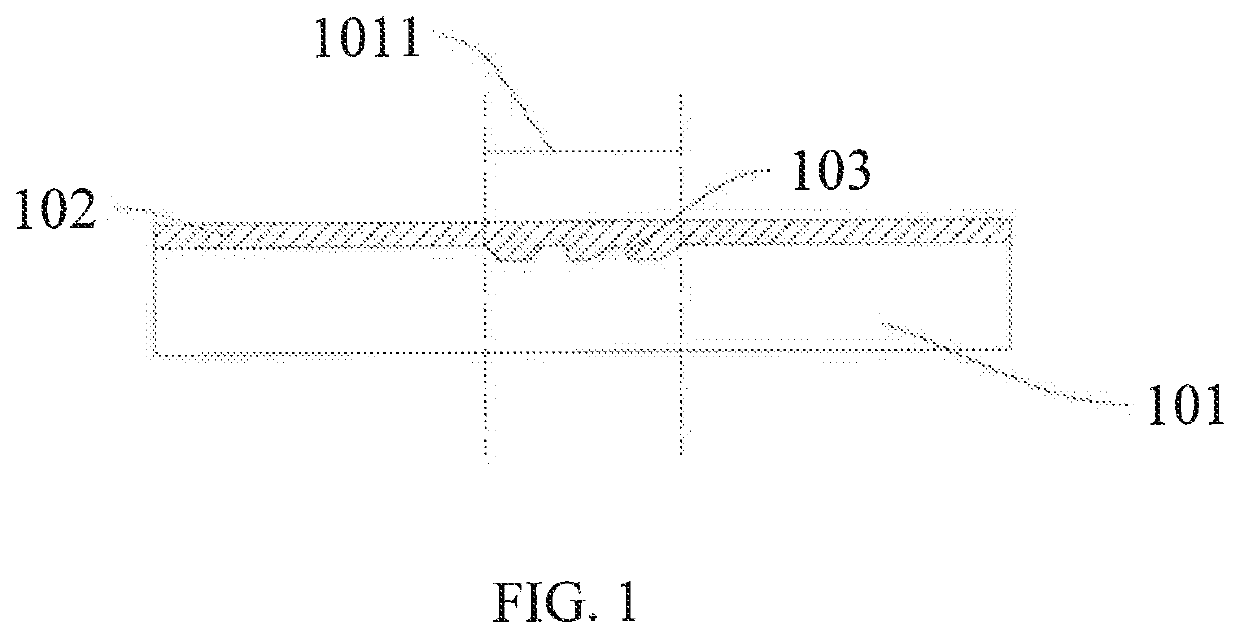
[0032]Please refer to FIG. 1. In a first embodiment, the present invention provides a display panel, including a bending area 1011. The display panel includes a first flexible substrate 101, a buffer layer 102 disposed on a surface of the first flexible substrate 101. A rough structure 103 is disposed on a surface of the first flexible substrate 101 in contact with the buffer layer 102 in the bending area 1011.

[0033]Specifically, the first flexible substrate 101 is made of polyimide. The buffer layer 102 is made of silicon dioxide. The surface of the first flexible substrate 101 in contact with the buffer layer 102 is treated, so that the rough structure 103 is formed on the surface of the first flexible substrate 101 in contact with the buffer layer 102. In a process of forming the rough structure 103, an imide bond in the polyimide is hydrolyzed to form a carboxylic acid group, and the carboxylic acid group is combined with the silicon dioxide in the buffer layer 102 to form a che...

second embodiment

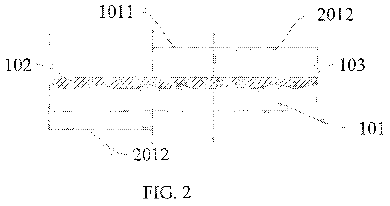
[0040]In the second embodiment, the rough structure is formed on the entire surface of the first flexible substrate of the display panel. By using roughness of the first flexible substrate, a surface bonding force between the first flexible substrate and the buffer layer can be increased, and a carboxylic acid group, referring to FIG. 5, is contained in the rough structure, wherein a chemical bond is formed between the carboxylic acid group and the silicon dioxide of the buffer layer to further increase the surface bonding force between the first flexible substrate and the buffer layer, thereby not only improving a situation of peeling of the first flexible substrate and the buffer layer in the bending area, but also avoiding a risk of peeling of the first flexible substrate in the non-bending area.

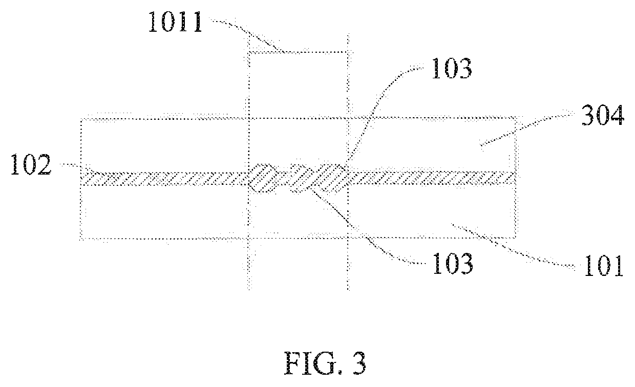
[0041]Please refer to FIG. 3. A display panel in accordance with a third embodiment of the present invention is different from the first embodiment in that the display panel further inclu...

third embodiment

[0045]the present invention may be implemented by another manner. Specifically, the display panel includes a first flexible substrate 101 and a second flexible substrate 304. The second flexible substrate 304 is disposed on a surface of the buffer layer 102 away from the first flexible substrate 101. In the bending area 1011 and the non-bending area 2012, each of surfaces of the first flexible substrate 101 and the second flexible substrate 304 in contact with the buffer layer 102 is provided with the rough structure 103.

[0046]In the third embodiment of the present invention, the display panel of has a two-layered flexible substrate structure, and the rough structure is also formed on the surface of the second flexible substrate in the bending area, or the rough structure is formed on the entire surface of the second flexible substrate. By using roughness of the second flexible substrate, a surface bonding force between the second flexible substrate and the buffer layer can be incre...


PUM


Abstract

A display panel and a method of manufacturing the same are disclosed. The display panel includes a bending area. The display panel includes a first flexible substrate. A buffer layer is disposed on a surface of the first flexible substrate. A rough structure is disposed on a surface of the first flexible substrate in contact with the buffer layer in the bending area.

Description

[0001]This application claims the priority of China Patent Application serial No. 201910730167.6, filed Aug. 8, 2019, titled “DISPLAY PANEL AND MANUFACTURING METHOD THEREOF”, the disclosures of which are incorporated herein by reference in their entirety.BACKGROUND OF INVENTION1. Field of Invention[0002]The present invention relates to a technical field of displays, and particularly to, a display panel and a manufacturing method thereof.2. Related Art[0003]Currently, most manufacturers use active-matrix organic light-emitting diode (AMOLED) technology based on flexible polyimide to achieve foldable and narrow bezel design displays. Polyimide has a characteristic of good flexibility, so it can be used for foldable products. By bending downward integrated circuit (IC) assembly areas of chip one Pi (COP) bonding areas of chip on film (COF) lower frames and part of wirings and circuits, lower frames of original rigid display panels can become smaller.[0004]However, in current display pa...

Claims


Application Information

Patent Timeline
IPC IPC(8): H01L51/00H01L27/32H01L51/56
CPCH01L51/0097H01L2227/323H01L51/56H01L27/3244H10K59/12H10K77/111Y02E10/549Y02P70/50H10K59/1201H10K2102/311G02F1/133305H01L33/12G09F9/301H01L33/22H01L33/24G06F1/1641G06F1/1652H10K71/00
Inventor HU, KAI
Owner WUHAN CHINA STAR OPTOELECTRONICS SEMICON DISPLAY TECH CO LTD
Why Eureka
Try Eureka