Electron emitting element

Active Publication Date: 2022-01-20
SHARP KK
View PDF4 Cites 1 Cited by
  • Summary
  • Abstract
  • Description
  • Claims
  • Application Information

AI Technical Summary

Benefits of technology

This patent relates to improving the performance of electron emitting elements by controlling the accumulation of conductive fine particles and reducing electron emission points. By forming an insulating layer that overlaps the electron emission region, a large number of electron emission points can be formed, resulting in improved electron emission characteristics. Additionally, the formation of current leakage paths inside the element can be suppressed, leading to a longer life of the electron emitting element.

Problems solved by technology

These agglomerates become current leakage paths inside the element, and may cause sudden interruptions in the function of the electron emitting element, or may lead to a reduction in the life of the electron emitting element.

Method used


Image

  • Electron emitting element
  • Electron emitting element
  • Electron emitting element

Examples


first embodiment

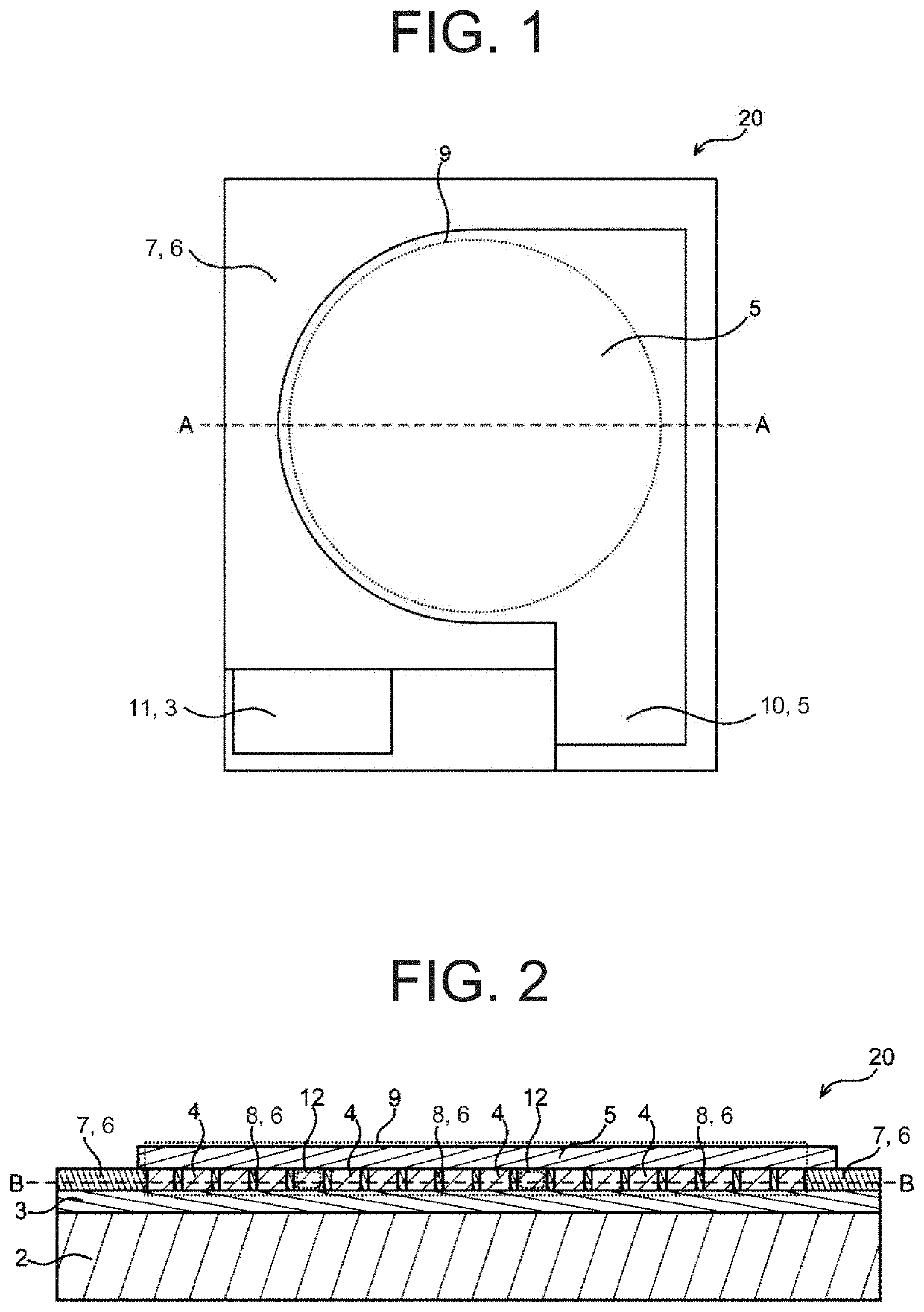
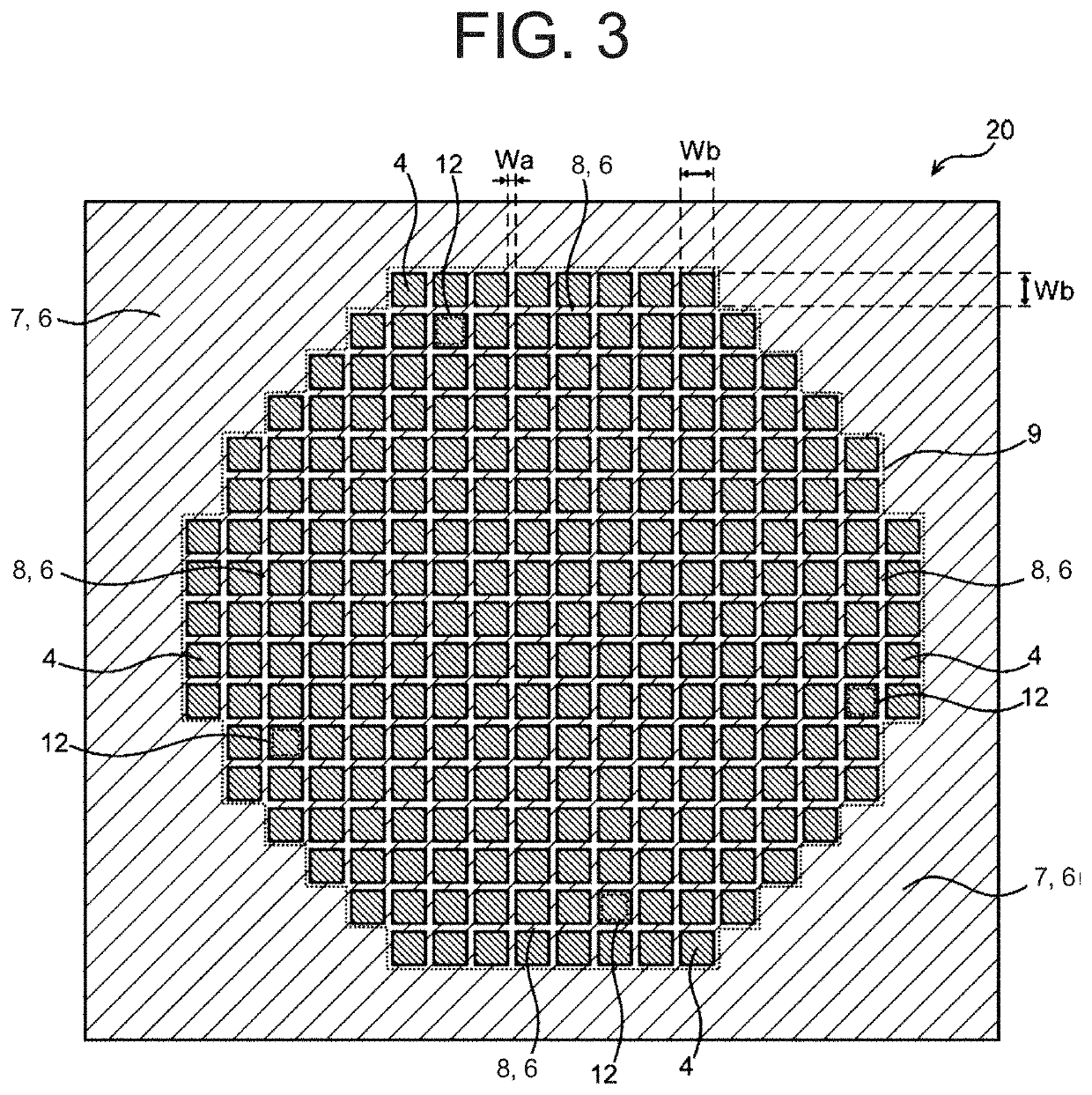
[0030]FIG. 1 is a plan view of an electron emitting element according to the present embodiment. FIG. 2 is a schematic cross-sectional view of the electron emitting element taken along the broken line A-A in FIG. 1. FIG. 3 is a schematic cross-sectional view of the electron emitting element taken along the broken line B-B in FIG. 2.

[0031]The electron emitting element 20 of the present embodiment includes a lower electrode 3, a surface electrode 5 facing the lower electrode 3, a resistance layer 4 arranged between the lower electrode 3 and the surface electrode 5, and an insulating layer 6 arranged between the lower electrode 3 and the surface electrode 5. The resistance layer 4 is an insulating resin layer containing conductive fine particles in a dispersed state. The lower electrode 3, the resistance layer 4, and the surface electrode 5 are provided such that electrons flow to the resistance layer 4 as a result of a potential difference being generated between the lower electrode 3...

second embodiment

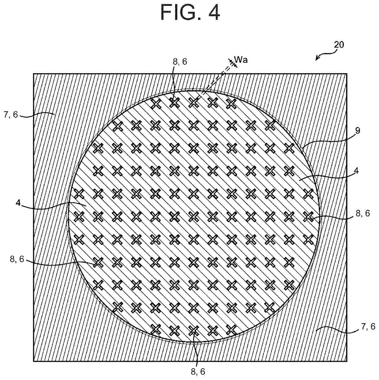
[0058]In the second embodiment, the overall shape of the insulating layer 6 constituting the emission control region 8 is a cross pattern. FIG. 4 is a schematic cross-sectional view of an electron emitting element according to the second embodiment. This cross-sectional view corresponds to the cross-sectional view shown in FIG. 3 of the first embodiment.

[0059]The emission control region 8 can have a pattern in which cross-shaped insulating layers 6 are evenly distributed in the electron emission region 9. In this way, by making the overall shape of the emission control region 8 a cross pattern, the overall length of the edges of the emission control region 8 can be made longer. Therefore, a large number of electron emission points can be formed in the electron emission region 9.

[0060]Furthermore, the overall shape of the emission control region 8 may be a shape that combines a lattice pattern as in the first embodiment and the cross pattern of the second embodiment.

[0061]The other c...

third embodiment

[0062]In the third embodiment, the overall shape of the insulating layer 6 constituting the emission control region 8 is a concentric circular shape. FIG. 5 is a schematic cross-sectional view of an electron emitting element according to the third embodiment. This cross-sectional view corresponds to the cross-sectional view shown in FIG. 3 of the first embodiment.

[0063]The emission control region 8 having a concentric circular shape can be provided so that the insulating layer 6 is evenly distributed in the electron emission region 9. In this way, by making the overall shape of the emission control region 8 a concentric circular shape, the overall length of the edges of the emission control region 8 can be made longer. Therefore, a large number of electron emission points can be formed in the electron emission region 9.

[0064]Furthermore, the overall shape of the emission control region 8 may be a shape that combines a lattice pattern as in the first embodiment and the concentric cir...


PUM


Abstract

This electron emitting element includes a lower electrode, a surface electrode facing the lower electrode, a resistance layer arranged between the lower electrode and the surface electrode, and an insulating layer arranged between the lower electrode and the surface electrode. The resistance layer is an insulating resin layer containing conductive fine particles in a dispersed state. The insulating layer has a peripheral region for defining the electron emission region, and an emission control region which is arranged so as to overlap the electron emission region defined by the peripheral region. The emission control region is configured by a line-shaped insulating layer, a plurality of dot-shaped insulating layers, or both a line-shaped insulating layer and a plurality of dot-shaped insulating layers. The percentage of an area that the emission control region represents within an area of an electron emission region defined by the peripheral region is 2% or more and 60% or less.

Description

BACKGROUND OF THE INVENTIONField of the Invention[0001]The present invention relates to an electron emitting element.Description of the Background Art[0002]An electron emitting element is known in which a resistance layer is provided between an electrode substrate and a surface electrode (for example, see Japanese Unexamined Patent Application Publication No. 2016-136485). A silicone resin layer containing silver nanoparticles is used as the resistance layer.[0003]In this electron emitting element, a current flows through the resistance layer due to an electric field generated by applying a voltage between the two electrodes. At this time, some of the electrons pass through the surface electrode and are emitted into the atmosphere and the like. Such an electron emitting element may be used as a charging device that charges a photosensitive body, a light emitting device, and the like.[0004]However, in the conventional electron emitting element, the silver nanoparticles can sometimes ...

Claims


Application Information

Patent Timeline
IPC IPC(8): H01J29/96H01J29/02
CPCH01J29/96H01J29/02H01J1/312H01J2201/30449H01J2201/3125H01J2201/3195
Inventor SHINKAWA, KOHJIIWAMATSU, TADASHIKOSAKA, TOMOHIROTSUJINO, KAZUYAABEYSINGHE, RESHAN MADUKA
Owner SHARP KK
Why Eureka
Try Eureka