Member for semicondutor manufacturing apparatus

a manufacturing apparatus and semiconductor technology, applied in the direction of ohmic resistance heating, hot plate heating arrangement, coating, etc., can solve the problems of reducing the resistance due to skin effect, increasing the temperature of the rf rod, so as to prevent the rf rod from heating each other, reduce the risk of breakage, and reduce the load of processing

Pending Publication Date: 2022-04-07
NGK INSULATORS LTD
View PDF0 Cites 1 Cited by
  • Summary
  • Abstract
  • Description
  • Claims
  • Application Information

AI Technical Summary

Benefits of technology

[0010]In the member for semiconductor manufacturing apparatus according to the present invention, the RF electrode may be provided across a plurality of planes at different heights within the ceramic plate. In this way, the density of the plasma can be changed for each plane of the RF electrode at a different height. In this case, each of the plurality of RF rods may be individually connected to one of the planes of the RF electrode. In this way, the distance between the RF rods can be ensured. For example, by increasing the distance between the RF rods that generate heat, it is possible to prevent the RF rods from heating each other. In addition, since the RF rods are connected to the RF electrode close to the back surface of the ceramic plate and the RE electrode far from the back surface of the ceramic plate, the depth of the hole of the RF rod connected to the RF electrode close to the back surface of the ceramic plate is small, which reduces the load of processing performed on the ceramic plate and reduces the risk of breakage. In contrast, when a plurality of the RF rods are connected to the RF electrode far from the back surface of the ceramic plate, the depth of the holes of the RF rods is large, which increases the load of processing performed on the ceramic plate and increases the risk of breakage.
[0011]In the member for semiconductor manufacturing apparatus according to the present invention, the plurality of RF rods may be merged into one rod in a second merged portion in front of the RF connector, and the one rod may be connected to the RF connector. In this way, when the RF link member is connected to the RE connector, the number of connection points between the RF link member and the RF connector can be reduced.
[0012]In the member for semiconductor manufacturing apparatus according to the present invention, the cross section obtained by cutting the RF rod in a direction perpendicular to the longitudinal direction of the RF rod may have a shape with at least one concave portion in the periphery of the shape. In this way, the surface area of the RF rod is increased, as compared with an RF rod without the concave portion, which decreases the increase in resistance due to the skin effect more. As a result, the amount of heat generated per RF rod is reduced more.
[0013]The member for semiconductor manufacturing apparatus according to the present invention may further include a resistance heating element embedded in the ceramic plate and a pair of heater rods that are connected to the resistance heating element and that extend through the hollow interior of the ceramic shaft to the outside of the ceramic shaft. The base end of the RF link member may be located at a position closer to the ceramic shaft than the base ends of the heater rods. In this way, the length of the part of the RF link member that generates heat is decreased, resulting in less heat generation. Furthermore, the work performed on the base end of the RF link member and the work performed on the base end of the heater rod are less likely to interfere with each other. As a result, each of the works can be smoothly performed. In addition, since the length of the RF link member can be relatively decreased, the resistance of the RF link member can be kept low, thus decreasing the amount of heat generated by the RF link member.
[0014]The member for semiconductor manufacturing apparatus according to the present invention may further include a resistance heating element embedded in the ceramic plate and a pair of heater rods that are connected to the resistance heating element and that extend through the hollow interior of the ceramic shaft to the outside of the ceramic shaft. The RF rod may be thicker than each of the heater rods. That is, it is desirable that the diameter of the RF rod be greater than that of the heater rod. This increases the surface area of the RF rods, which decreases the resistance of the RF current flowing through the RF rods. As a result, the amount of heat generated per RF rod is reduced more. Note that when the member for semiconductor manufacturing apparatus has the first merged portion, it is desirable that the diameter of the first merged portion be greater than that of the heater rod. When the member for semiconductor manufacturing apparatus has the second merged portion, it is desirable that the diameter of the second merged portion be greater than that of the heater rod.

Problems solved by technology

However, when an RF connector is disposed in the hollow interior of the ceramic shaft as in PTL 1, the temperature in the hollow interior of the ceramic shaft may increase due to the heat generated by the RF connector.
In such a case, even if the amount of heat generated by the RF rod is small, the temperature of the RF rod is likely to rise, and a hot spot may occur in the ceramic plate.
This increases the surface area of the current flow path of the RF link member, thus decreasing the increase in resistance due to the skin effect.

Method used


Image

  • Member for semicondutor manufacturing apparatus
  • Member for semicondutor manufacturing apparatus
  • Member for semicondutor manufacturing apparatus

Examples


Embodiment Construction

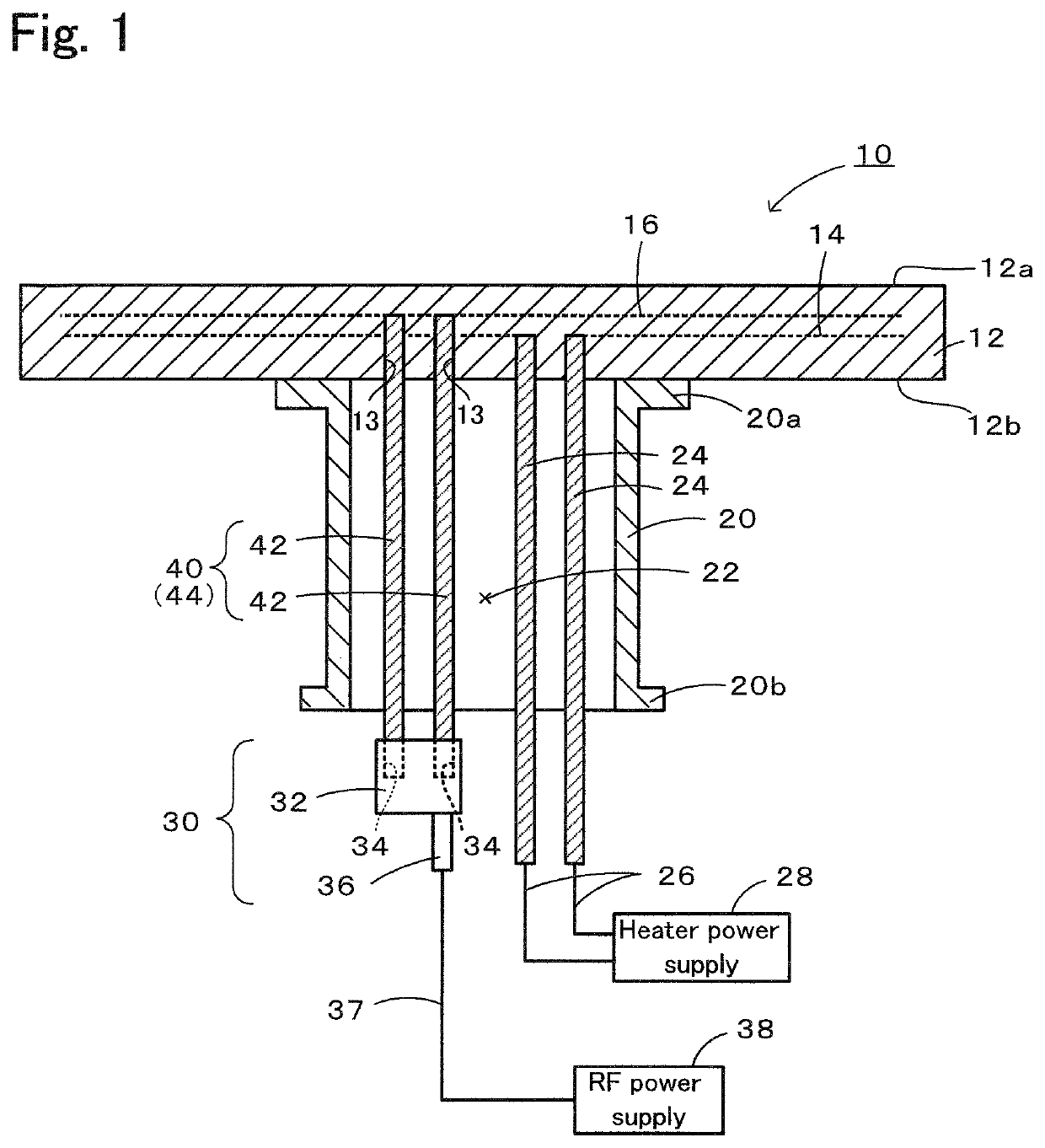
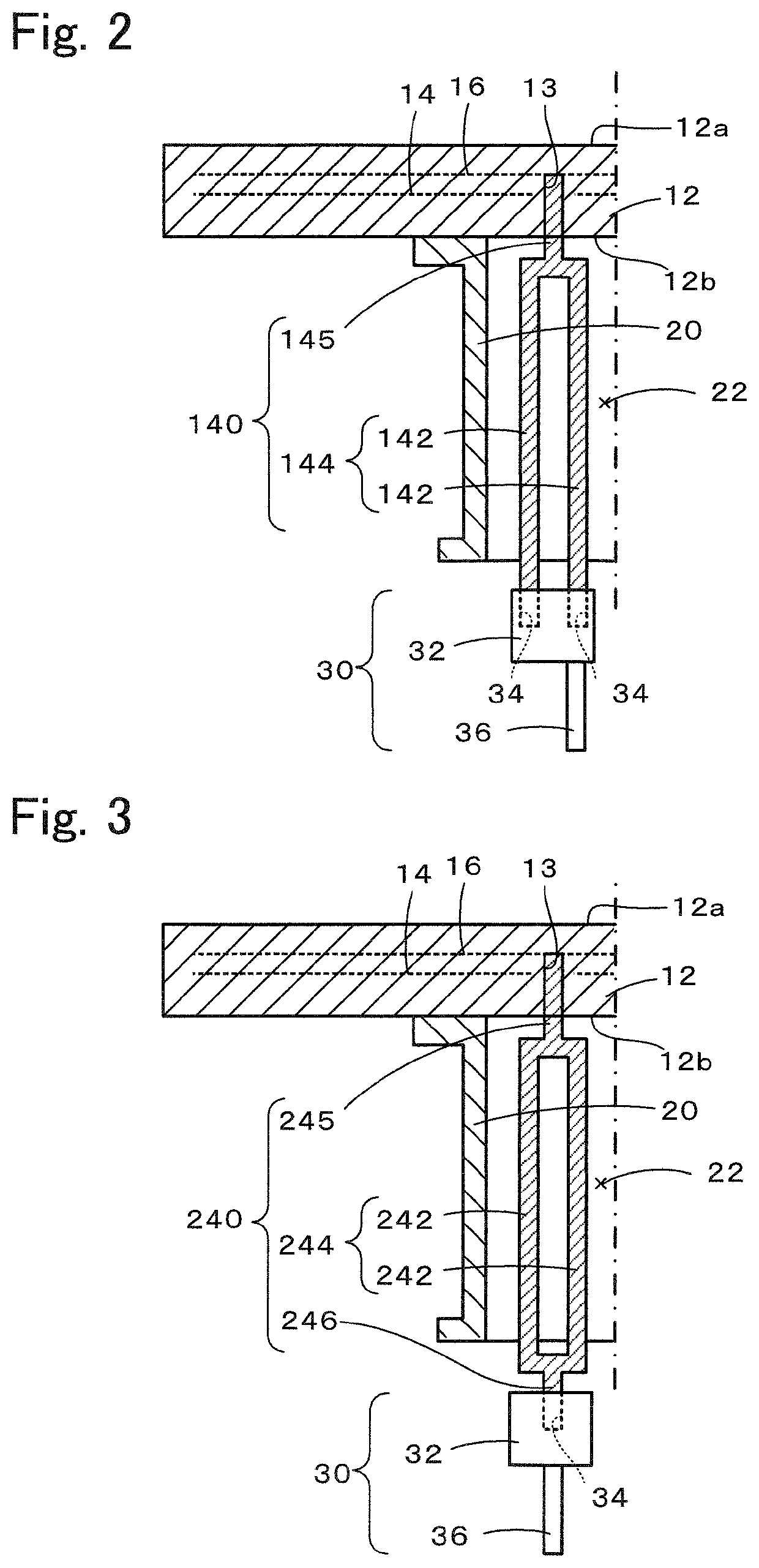
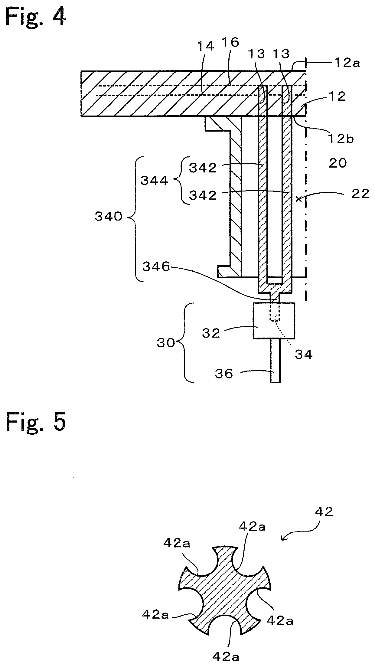
[0021]An exemplary embodiment of the present invention is described below with reference to the accompanying drawings. FIG. 1 is a longitudinal sectional view of a ceramic heater 10.

[0022]Note that the terms “up” and “down” as used in the specification are intended to indicate a relative positional relationship, not an absolute positional relationship. Accordingly, the terms “up” and “down” may change to “down” and “up”, “left” and “right”, or “front” and “rear”, respectively, depending on the orientation of the ceramic heater 10.

[0023]The ceramic heater 10 is one of the members for semiconductor manufacturing apparatus. The ceramic heater 10 is used to support and heat a wafer to be processed through, for example, CVD or etching using plasma. The ceramic heater 10 is installed inside a chamber for a semiconductor process (not illustrated). The ceramic heater 10 includes a ceramic plate 12, a ceramic shaft 20, heater rods 24, an RF connector 30, and an RF link member 40.

[0024]The ce...


PUM

PropertyMeasurementUnit
temperatureaaaaaaaaaa
heightsaaaaaaaaaa

Abstract

A member for semiconductor manufacturing apparatus has a structure in which a hollow ceramic shaft is provided on a back surface of a ceramic plate having a front surface serving as a wafer placement surface. The member for semiconductor manufacturing apparatus includes an RF electrode embedded in the ceramic plate, an RF connector disposed outside of the hollow interior of the ceramic shaft, and an RF link member provided between the RF connector and the RF electrode. The RF link member has a branching portion consisting of a plurality of RF rods, and the branching portion extends to the outside of the ceramic shaft.

Description

BACKGROUND OF THE INVENTION1. Field of the Invention[0001]The present invention relates to a member for semiconductor manufacturing apparatus.2. Description of the Related Art[0002]In some semiconductor manufacturing apparatuses, such as etching apparatuses and CVD apparatuses, there has been used a member for semiconductor manufacturing apparatus having a structure in which a cylindrical ceramic shaft is connected to a back surface of a disk-shaped ceramic plate having a front surface serving as a wafer placement surface. Some of the members for semiconductor manufacturing apparatus have a high-frequency electrode (an RF electrode) embedded in a ceramic plate and generates plasma by using the RF electrode. For example, in a member for semiconductor manufacturing apparatus described in PTL 1, a plurality of RF rods are connected to an RF electrode, and the plurality of RF rods branch off from a single RF connector disposed in the hollow interior of the ceramic shaft. Since in PTL 1,...

Claims


Application Information

Patent Timeline
Patent Type & Authority Applications(United States)
IPC IPC(8): H01L21/683
CPCH01L21/6833H01J37/32724H01L21/3065H05B3/74C23C16/509C23C16/4581C23C16/46H01L21/67103H05B2203/016H05B3/283H01L21/68792H01L21/68757H05B3/748H01L21/67069H01J37/32577C23C16/4586H01J2237/2007
Inventor TAMURA, RYUJI
Owner NGK INSULATORS LTD
Why Eureka
Try Eureka