Semiconductor device

Active Publication Date: 2022-04-07
MITSUBISHI ELECTRIC CORP
View PDF3 Cites 0 Cited by
  • Summary
  • Abstract
  • Description
  • Claims
  • Application Information

AI Technical Summary

Benefits of technology

The present invention provides a semiconductor device that reduces the likelihood of a drop in reverse bias safe operating area, which means the device can handle higher voltages without being damaged. This is achieved by using a specific layout design that reduces the likelihood of latching up and minimizes the flow of hole current. Additionally, the design helps to efficiently extract holes in the outer peripheral region near the transistor region, which helps to further reduce the likelihood of a reverse bias safe operating area drop.

Problems solved by technology

This RC-IGBT has some technical problems, one of which is that the recovery loss during the operation of the diode is large.
However, when the concentration of p-type impurities in an anode region is high, the existence of a large amount of excess carriers makes it difficult for the carriers inside the device to be discharged.
Therefore, there has been a problem that the recovery loss is increased.
In the disclosure of Japanese Patent Application Laid-Open No. 2017-224685, no countermeasure is taken against the inflow of holes from the outer peripheral region having a deep p-type diffusion layer whose concentration is generally high, so that the countermeasure against a drop in a reverse bias safe operating area (RBSOA) is insufficient.

Method used


Image

  • Semiconductor device
  • Semiconductor device
  • Semiconductor device

Examples


first preferred embodiment

[0045]

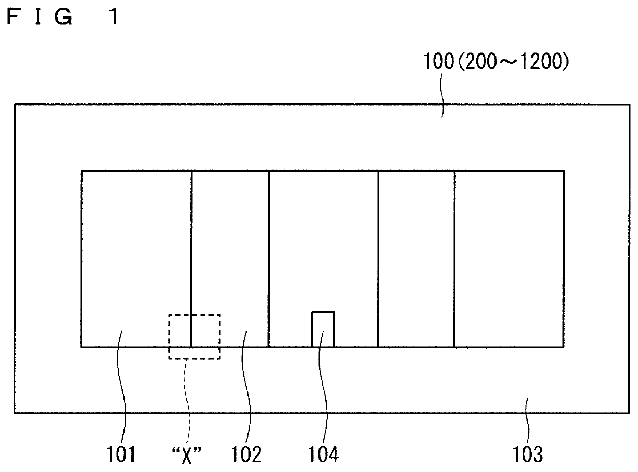
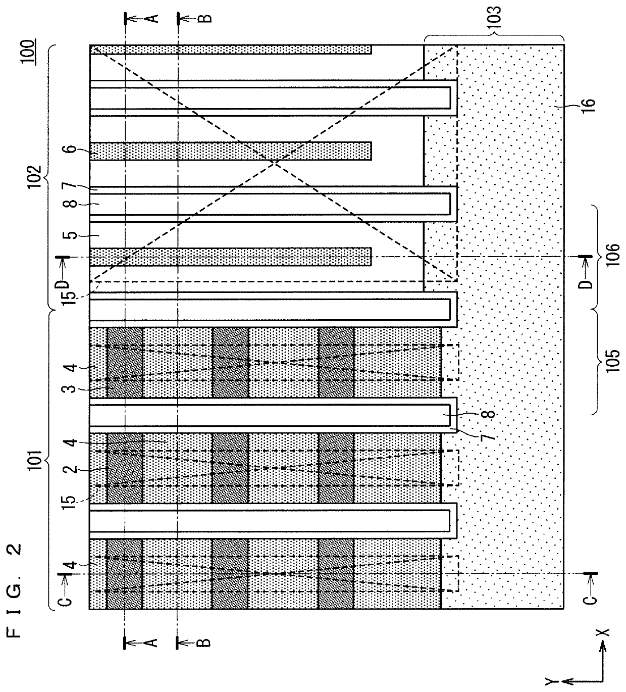
[0046]FIG. 1 is a plan view illustrating an entire chip of an RC-IGBT 100 according to a first preferred embodiment, and FIG. 2 is a plan view illustrating a region X surrounded by the dashed line in FIG. 1. The RC-IGBT 100 illustrated in FIG. 1 has IGBT regions 101 (transistor regions) and FWD regions 102 (diode regions) arranged side by side in a stripe shape, which is referred to as a “stripe type”.

[0047]As illustrated in FIG. 1, an outer peripheral region 103 is provided to surround the IGBT regions 101 and the FWD regions 102, and one of the IGBT regions 101 is partially provided with a gate pad region 104. It should be noted that the plan view illustrating the entire chip is also the same in each of RC-IGBTs 200 to 1200 of the second to twelfth preferred embodiments described later.

[0048]As illustrated in FIG. 2, the IGBT region 101 is divided into a plurality of IGBT unit cell regions 105 (transistor unit cell regions) by a plurality of embedded gate electrodes 8 each h...

second preferred embodiment

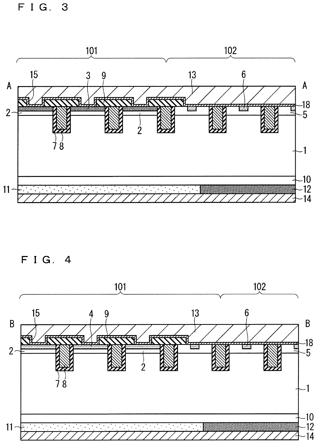
[0095]Next, an RC-IGBT 200 according to a second preferred embodiment will be described with reference to FIGS. 7 to 10. A plan view illustrating an entire chip of the RC-IGBT 200 is the same as FIG. 1, and FIG. 7 is a plan view illustrating the region X surrounded by the dashed line in FIG. 1. A cross-sectional view taken along the A-A line illustrated in FIG. 7 and viewed from the direction indicated by the arrows is illustrated in FIG. 8, a cross-sectional view taken along the B-B line and viewed from the direction indicated by the arrows is illustrated in FIG. 9, a cross-sectional view taken along the C-C line and viewed from the direction indicated by the arrows is illustrated in FIG. 10, and a cross-sectional view taken along the D-D line and viewed from the direction indicated by the arrows is illustrated in FIG. 11. In FIGS. 7 to 10, the same configurations as those of the RC-IGBT 100 described with reference to FIGS. 2 to 6 are designated by the same reference numerals, and...

third preferred embodiment

[0099]Next, an RC-IGBT 300 according to a third preferred embodiment will be described with reference to FIGS. 12 to 16. A plan view illustrating an entire chip of the RC-IGBT 300 is the same as FIG. 1, and FIG. 12 is a plan view illustrating the region X surrounded by the dashed line in FIG. 1. A cross-sectional view taken along the A-A line illustrated in FIG. 12 and viewed from the direction indicated by the arrows is illustrated in FIG. 13, a cross-sectional view taken along the B-B line and viewed from the direction indicated by the arrows is illustrated in FIG. 14, a cross-sectional view taken along the C-C line and viewed from the direction indicated by the arrows is illustrated in FIG. 15, and a cross-sectional view taken along the D-D line and viewed from the direction indicated by the arrows is illustrated in FIG. 16. In FIGS. 12 to 16, the same configurations as those of the RC-IGBT 100 described with reference to FIGS. 2 to 6 are designated by the same reference numerals...


PUM


Abstract

A semiconductor substrate has a transistor region, a diode region, and an outer peripheral region. The transistor region is divided into a plurality of transistor unit cell regions by a plurality of gate electrodes each having a stripe shape, and the diode region is divided into a plurality of diode unit cell regions by the plurality of gate electrodes. Each of the plurality of transistor unit cell regions has a third semiconductor layer of a first conductivity type provided on a first main surface side of the semiconductor substrate, a fourth semiconductor layer of a second conductivity type selectively provided on an upper layer part of the third semiconductor layer, and a fifth semiconductor layer.The fifth semiconductor layer is provided to be in contact with an impurity layer of the first conductivity type provided in the outer peripheral region, or to enter the impurity layer.

Description

BACKGROUND OF THE INVENTIONField of the Invention[0001]The present disclosure relates to a semiconductor device, and relates to a semiconductor device having a reduced recovery loss.Description of the Background Art[0002]In general, power devices are required to meet various requirements such as withstand voltage holding capacity and guarantee of a safe operating area so that the device does not break during its operation. One of the requirements is low loss. Reducing loss in power devices has the effects of reducing the size and weight of the device, and in a broad sense, it has an effect that leads to the conservation of the global environment by reducing energy consumption. It is further required to realize a power device that achieves these effects at the lowest possible cost.[0003]As means for meeting the above requirements, an RC-IGBT (Reverse-Conducting Insulated Gate Bipolar Transistor) that achieves the characteristics of an IGBT and an FWD (Free Wheeling Diode) by one stru...

Claims


Application Information

Patent Timeline
IPC IPC(8): H01L29/06H01L27/07H01L29/739H01L29/861
CPCH01L29/0634H01L27/0727H01L29/0696H01L29/861H01L29/7397H01L29/8613H01L29/407H01L29/1608H01L29/0692H01L29/1095H01L29/0834H01L29/0619H01L29/0638H01L29/402H01L29/4238
Inventor TAKAHASHI, TETSUOFUJII, HIDENORIHONDA, SHIGETO
Owner MITSUBISHI ELECTRIC CORP
Why Eureka
Try Eureka