Semiconductor structure formation method and mask

a technology of semiconductor structure and mask, which is applied in the field of semiconductor structure formation method and mask, can solve the problems of increasing difficulty and complexity of manufacturing ics, and the difficulty of increasing the matching degree between the pattern formed on the wafer and the target pattern, and achieves the effect of high density, easy to meet the requirements of photolithography process, and large siz

Pending Publication Date: 2022-04-28
SEMICON MFG INT (SHANGHAI) CORP +1
View PDF6 Cites 2 Cited by
  • Summary
  • Abstract
  • Description
  • Claims
  • Application Information

AI Technical Summary

Benefits of technology

[0029]In forms of the semiconductor structure formation method provided in the the present disclosure, the ion doping is performed on the mandrel material layer in the second region to form the anti-etching layer located in the second region and the mandrel layer located in the first region. In the step of forming the first trench, part of the mandrel material layer in the first region remains at two sides of the first trench along the second direction, that is to say, the first region spans the first trench along the second direction. Then the spacers are formed on the side walls of the first trench, so that the spacers form the first groove by encircling. In the step of removing the mandrel layer, the formed second grooves are correspondingly located at two sides of the first groove, and the first groove and the second groove are spaced apart by the spacer. In forms of the present disclosure, compared with the second groove, the first region is bigger in size, and therefore is easy to meet requirements of a photolithography process. Besides, the first region except an overlap between the first region and the first trench is used for defining the shape and size of the second groove, so that by using the overlap between the pattern of the first region and the pattern of the first trench, the second groove can be smaller in size. A space between the second groove and the first groove is defined by the thickness of the spacer. One can satisfy the design of the smallest space between the first groove and the second groove, facilitating, without changing limiting conditions of the photolithography process, implementation of a smaller critical dimension of the target pattern and further compression of a pitch between the target patterns, to meet requirements of the high density and high integration of an IC. Besides, with reasonable alteration on the existing process, the process is low in complexity and is highly friendly to the photolithography process.

Problems solved by technology

In the development process of ICs, generally, as a functional density (that is, a quantity of interconnection structures per chip) gradually increases, a geometric size (that is, the smallest component size that can be produced by using process steps) gradually decreases, which correspondingly increases a difficulty and complexity of manufacturing ICs.
Currently, as technological nodes become increasingly small, how to increase a matching degree between a pattern formed on a wafer and a target pattern has become a challenge.

Method used


Image

  • Semiconductor structure formation method and mask
  • Semiconductor structure formation method and mask
  • Semiconductor structure formation method and mask

Examples


Embodiment Construction

[0041]It can be seen from the related art, as technological nodes become increasingly small, it becomes challenging to enable a pattern formed on a wafer to better match a target pattern.

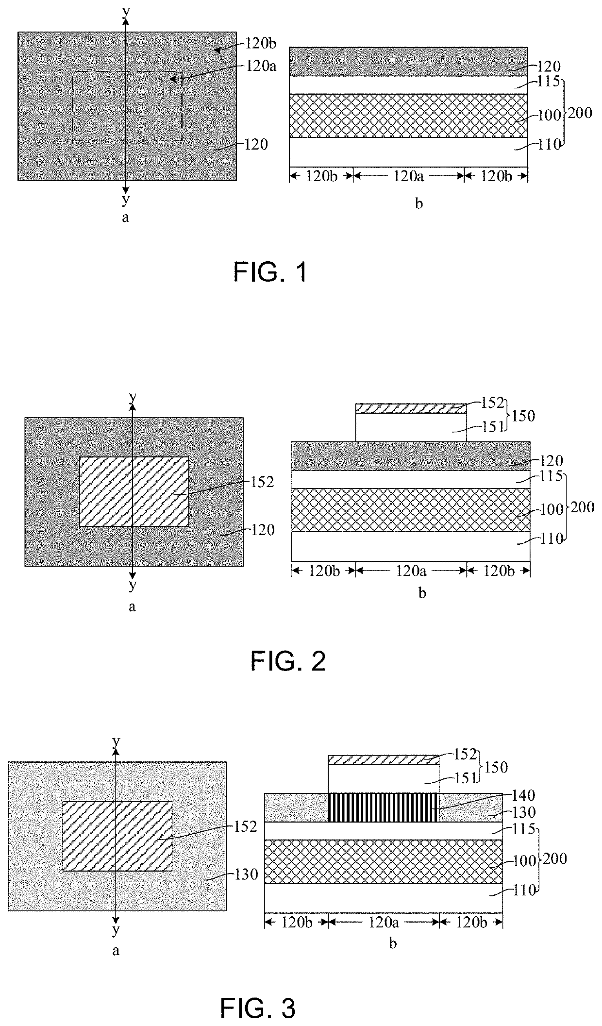
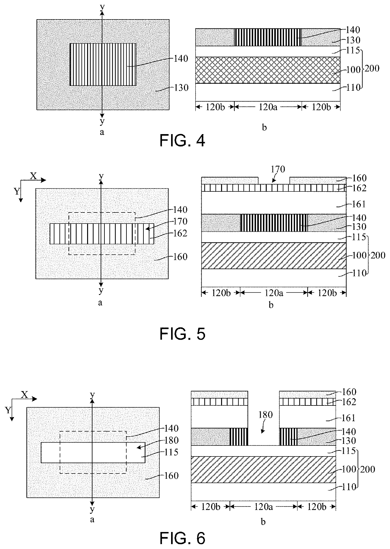
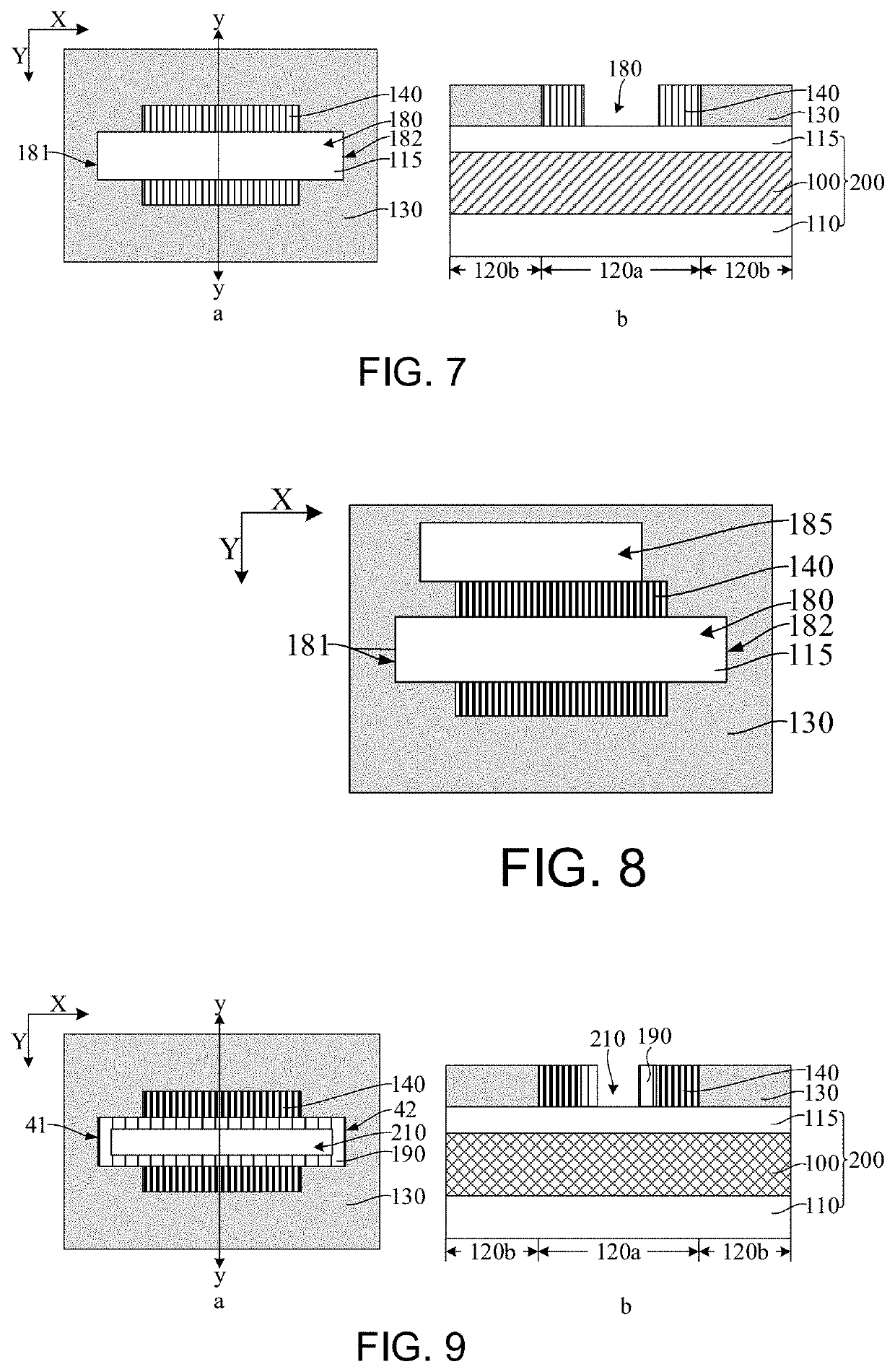
[0042]To address the foregoing technical problems, embodiments and implementations of the present disclosure provide forms of a semiconductor structure formation method, in which ion doping is performed on a mandrel material layer in a second region to form an anti-etching layer located in the second region and a mandrel layer located in a first region. In a step of forming a first trench, part of the mandrel material layer in the first region remains at two sides of the first trench along a second direction, that is to say, the first region spans the first trench along the second direction. Then spacers are formed on side walls of the first trench, so that the spacers form a first groove by encircling it. In a step of removing the mandrel layer, formed second grooves are correspondingly located at ...


PUM

PropertyMeasurementUnit
semiconductor structure formation methodaaaaaaaaaa
etching resistanceaaaaaaaaaa
semiconductoraaaaaaaaaa

Abstract

A semiconductor structure formation method and a mask are provided. One form of the formation method includes: providing a base, including a target layer; forming a mandrel material layer on the base, the mandrel material layer including a first region and a second region encircling the first region; performing ion doping on the mandrel material layer in the second region, the ion doping being suitable for increasing the etching resistance of the mandrel material layer, where the mandrel material layer in the second region serves as an anti-etching layer, and the mandrel material layer in the first region serves as a mandrel layer; forming a first trench that runs through, along a first direction, at least part of the mandrel material layer in the first region, where part of the mandrel material layer in the first region remains at two sides of the first trench along a second direction; forming spacers on side walls of the first trench, so that the spacers form a first groove by encircling; removing the mandrel layer to form second grooves; and etching, using the anti-etching layer and the spacers as masks, the target layer below the first groove and the second grooves, to form the target pattern. In embodiments and implementations of the present disclosure, a pitch between target patterns is further compressed.

Description

RELATED APPLICATIONS[0001]The present application claims priority to Chinese Patent Appln. No. 202011137109.1, filed Oct. 22, 2020, the entire disclosure of which is hereby incorporated by reference.BACKGROUNDTechnical Field[0002]Embodiments of the present disclosure relate to the field of semiconductor manufacturing, and in particular, to a semiconductor structure formation method and a mask.Related Art[0003]With the rapid growth of the semiconductor integrated circuit (IC) industry, semiconductor technology continues to develop toward smaller process nodes driven by Moore's Law, such that ICs develop toward a direction of smaller size, higher circuit precision, and higher circuit complexity.[0004]In the development process of ICs, generally, as a functional density (that is, a quantity of interconnection structures per chip) gradually increases, a geometric size (that is, the smallest component size that can be produced by using process steps) gradually decreases, which correspond...

Claims


Application Information

Patent Timeline
Patent Type & Authority Applications(United States)
IPC IPC(8): H01L21/033H01L21/311H01L21/768
CPCH01L21/0337H01L21/31155H01L21/76816H01L21/31144H01L2221/101H01L21/32155H01L21/32134H01L21/0332H01L21/3215
Inventor JIN, JISONG
Owner SEMICON MFG INT (SHANGHAI) CORP
Why Eureka
Try Eureka