Self-Selective Multi-Terminal Memtransistor for Crossbar Array Circuits

a cross-bar array circuit and multi-terminal technology, applied in the field of self-selective multi-terminal memtransistor, can solve the problems of limiting the size of the array, affecting the performance of the array, and affecting the data rate and energy consumption of the system, so as to achieve linear and symmetric synaptic weight updating, not consuming a lot of power, and suppressing the leakage current of the sneak path

Pending Publication Date: 2022-05-12
NAT UNIV OF SINGAPORE
View PDF0 Cites 0 Cited by
  • Summary
  • Abstract
  • Description
  • Claims
  • Application Information

AI Technical Summary

Benefits of technology

[0012]A first advantage of embodiments of a device and circuit in accordance with the invention is that in operation, the memtransistor does not consume a lot of power as it has a low switching voltage of about 0.42 Volts and a switching energy of about 20 fJoules / bit.
[0013]A second advantage of embodiments of a device and circuit in accordance with the invention is that the memtransistors may be independently controlled by varying the voltage applied to the gate terminal of the memtransistor.
[0014]A third advantage of embodiments of a device and circuit in accordance with the invention is that the sneak current between adjacent memtransistors in the crossbar array is minimized, to less than 0.1 Nano-Amperes.
[0015]A fourth advantage of embodiments of a device and circuit in accordance with the invention is that when the gate terminals of each memtransistor in the same row are connected to form word lines in the crossbar array circuit, these gate terminals serve as natural selectors to enable multibit data storage, suppress sneak path leakage current and realize linear and symmetric synaptic weight updating.
[0016]A fifth advantage of embodiments of a circuit in accordance with the invention is that the circuit architecture is capable of performing multiply-and-accumulate operations to solve data-centric tasks in pattern recognition, which could be extended to other AI-driven applications such as speech recognition, autonomous vehicles, among others.
[0017]A sixth advantage of embodiments of a device in accordance with the invention is that through the use of a three-terminal architecture that has an electrostatic gate effect, this provides an additional knob to effectively suppress sneak current, enable a linear and symmetry synaptic plasticity, and a practical readout margin for gigabit-scale integration.

Problems solved by technology

However, the conventional von Neumann architecture which physically separates the processing and memory units presently suffers from a fundamental limitation in its data rate and energy consumption due to the enormous movement of data between both subsystems.
However, the high sneak current that flows through the neighbouring memory cells remains a fundamental issue.
However, this limits the size of the array as the performance requirement for the memristor and selector is very demanding.
Thus, despite being a three-terminal device, the gate control is still not able to provide the required additional selection function to avoid crosstalk issues from occurring between neighbouring cells.
Based on these values, it can be seen that this circuit design and configuration consumes a significant amount of power.
Even though these steps were taken, the switching energy of the proposed circuit design was still much larger than Nano-Joules and as a result, this design was unable to meet the low-power consumption requirement of in memory computing.

Method used


Image

  • Self-Selective Multi-Terminal Memtransistor for Crossbar Array Circuits
  • Self-Selective Multi-Terminal Memtransistor for Crossbar Array Circuits
  • Self-Selective Multi-Terminal Memtransistor for Crossbar Array Circuits

Examples


first embodiment

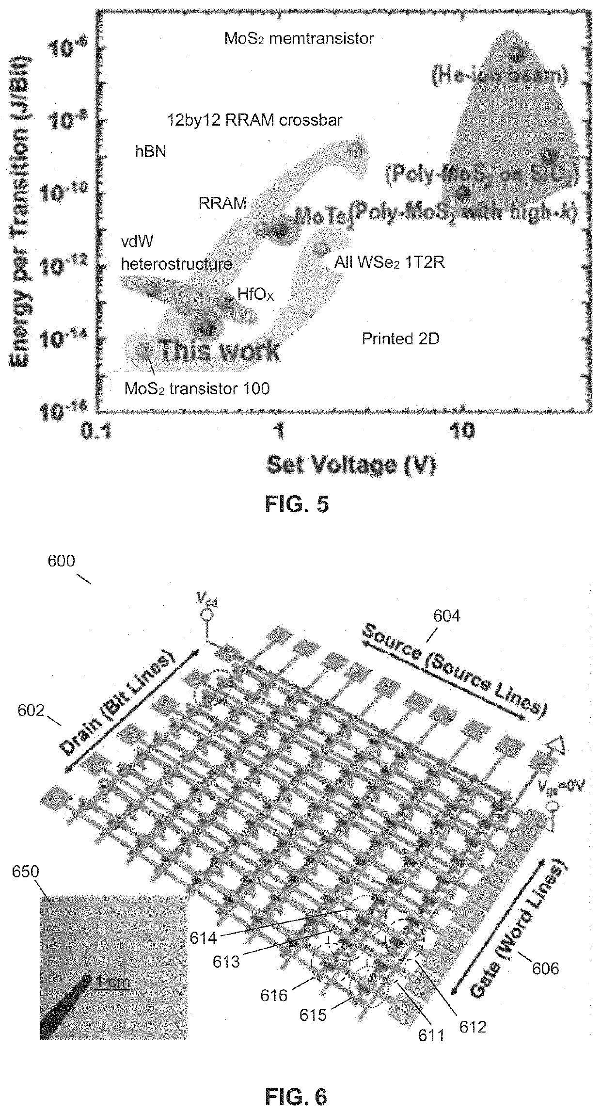
[0080]In the crossbar array circuit, the crossbar array circuit may comprise of a first 611 and a second 612 memtransistor whereby each memtransistor has the same structure as memtransistor 100. The drain electrodes of the first 611 and second 612 memtransistors may be electrically connected to a first bit line terminal, a gate electrode of the first 611 memtransistor may be electrically connected to a first gate terminal, a gate electrode of the second 612 memtransistor may be electrically connected to a second gate terminal, and the source electrodes of the first 611 and second 612 memtransistors may be electrically connected to a first source line terminal.

second embodiment

[0081]In the crossbar array circuit, in addition to the circuit comprising the first 611 and second 612 memtransistors, the circuit may further comprise a third 613 and a fourth 614 memtransistor whereby each memtransistor has the same structure as memtransistor 100. The drain electrodes of the third 613 and fourth 614 memtransistors may be electrically connected to the first bit line terminal, a gate electrode of the third 613 memtransistor may be electrically connected to the first gate terminal, a gate electrode of the fourth 614 memtransistor may be electrically connected to the second gate terminal, and source electrodes of the third 613 and fourth 614 memtransistors may be electrically connected together to a second source line terminal.

third embodiment

[0082]In the crossbar array circuit, the circuit may comprise a fifth 615 and a sixth 616 memtransistor whereby each memtransistor has the same structure as memtransistor 100. The drain electrodes of the fifth 615 and sixth 616 memtransistors may be electrically connected to a second bit line terminal, gate electrodes of the fifth 615 and sixth 616 memtransistors may be electrically connected to a third gate terminal, a source electrode of the fifth 615 memtransistor may be electrically connected to a third source line terminal, and a source electrode of the sixth 616 memtransistor may be electrically connected to a fourth source line terminal.

[0083]One skilled in the art will recognize that the first, second and third embodiments of the crossbar array circuit may be combined together as required without departing from the invention. FIG. 6 illustrates a three-dimensional schematic of a 10×10 MoS2 crossbar array 600 made up of memtransistors 100. As shown, it can be seen that the dr...


PUM

PropertyMeasurementUnit
switching voltageaaaaaaaaaa
temperatureaaaaaaaaaa

Abstract

This disclosure describes a self-selective multi-terminal memtransistor suitable for use in crossbar array circuits. In particular, the memtransistor comprises a sapphire substrate that has a single-layer of polycrystalline molybdenum disulphide (MoS2) thin film formed on the surface of the substrate, wherein the MoS2 thin film comprise MoS2 grains that are oriented along terraces provided on the surface of the substrate. The memtransistor has a drain electrode and a source electrode that is formed on the MoS2 thin film such that a channel is defined in the MoS2 thin film between the drain and source electrodes, and a gate electrode formed above the channel, whereby the gate electrode is isolated from the channel by a gate dielectric layer.

Description

CROSS-REFERENCE TO RELATED APPLICATION[0001]This application claims the benefit of Singapore Patent Application No. 10202011172S, filed on 10 Nov. 2020. The entire contents of which is incorporated herein by reference.FIELD OF THE INVENTION[0002]This invention relates to a self-selective multi-terminal memtransistor suitable for use in crossbar array circuits. In particular, the memtransistor comprises a sapphire substrate that has a single-layer of polycrystalline molybdenum disulphide (MoS2) thin film formed on the surface of the substrate, wherein the MoS2 thin film comprise MoS2 grains that are oriented along terraces provided on the surface of the substrate. The memtransistor has a drain electrode and a source electrode that is formed on the MoS2 thin film such that a channel is defined in the MoS2 thin film between the drain and source electrodes, and a gate electrode formed above the channel, whereby the gate electrode is isolated from the channel by a gate dielectric layer.S...

Claims


Application Information

Patent Timeline
Patent Type & Authority Applications(United States)
IPC IPC(8): H01L27/24G11C13/00H01L45/00
CPCH01L27/2481H01L45/16H01L45/1206G11C13/0002G11C13/003G11C2213/77G11C2213/53G11C13/0069G11C2013/0078G11C2213/15G11C11/56G11C11/54H10B63/80H10N70/253H10N70/24H10N70/823H10N70/8822H10N70/023H10B63/84H10N70/011
Inventor FENG, XUEWEIANG, KAH WEE
Owner NAT UNIV OF SINGAPORE
Why Eureka
Try Eureka