Heat treatment method and heat treatment apparatus

a heat treatment method and heat treatment technology, applied in the direction of optical radiation measurement, semiconductor/solid-state device testing/measurement, instruments, etc., can solve the problems of affecting the formation of good devices and the inability to reduce the depth of the junction

Pending Publication Date: 2022-06-02
DAINIPPON SCREEN MTG CO LTD
View PDF0 Cites 1 Cited by
  • Summary
  • Abstract
  • Description
  • Claims
  • Application Information

AI Technical Summary

Benefits of technology

[0019]According to the heat treatment method according to the first aspect, when a front-surface temperature of the substrate measured by the radiation thermometer reaches the target temperature, the supply of a current to the flash lamp is stopped to lower the front-surface temperature of the substrate, so that the front-surface temperature of the substrate can be accurately raised to the target temperature regardless of the front-surface state of the substrate.
[0020]According to the heat treatment method according to the second to fifth aspects, the scheduled arrival time at which the front-surface temperature of the substrate reaches the target temperature is predicted from the temperature measurement result by the radiation thermometer, and the supply of a current to the flash lamp is stopped within the predetermined period including the scheduled arrival time to lower the front-surface temperature of the substrate, so that the front-surface temperature of the substrate can be accurately raised to the target temperature regardless of the front-surface state of the substrate.
[0021]According to the heat treatment apparatus according to the sixth aspect, when a front-surface temperature of the substrate measured by the radiation thermometer reaches the target temperature, the supply of a current to the flash lamp is stopped to lower the front-surface temperature of the substrate, so that the front-surface temperature of the substrate can be accurately raised to the target temperature regardless of the front-surface state of the substrate.
[0022]According to the heat treatment apparatus according to the seventh to tenth aspects, the scheduled arrival time at which the front-surface temperature of the substrate reaches the target temperature is predicted from the temperature measurement result by the radiation thermometer, and the supply of a current to the flash lamp is stopped within the predetermined period including the scheduled arrival time to lower the front-surface temperature of the substrate, so that the front-surface temperature of the substrate can be accurately raised to the target temperature regardless of the front-surface state of the substrate.

Problems solved by technology

On this occasion, when the annealing time is about several seconds or more, the impurities driven in are deeply diffused by heat, and as a result, the junction depth may become too large as compared with the required depth, which may hinder the formation of a good device.

Method used


Image

  • Heat treatment method and heat treatment apparatus
  • Heat treatment method and heat treatment apparatus
  • Heat treatment method and heat treatment apparatus

Examples


first embodiment

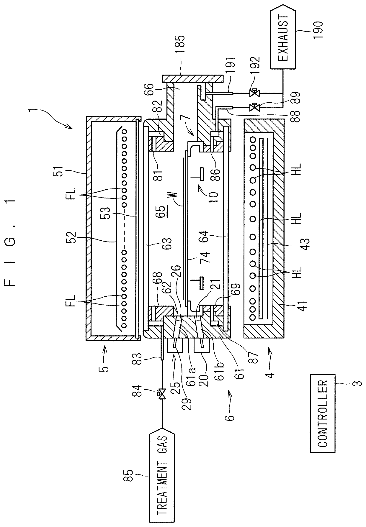
[0039]FIG. 1 is a longitudinal sectional view showing a configuration of a heat treatment apparatus 1 according to the present invention. The heat treatment apparatus 1 of FIG. 1 is a flash lamp annealer for irradiating a disk-shaped semiconductor wafer W serving as a substrate with flashes of light to heat the semiconductor wafer W. The size of the semiconductor wafer W to be treated is not particularly limited, and has a diameter of, for example, 300 mm or 450 mm (300 mm in the present embodiment). The semiconductor wafer W before being carried into the heat treatment apparatus 1 is implanted with impurities, and the activation treatment of impurities implanted by heating treatment with the heat treatment apparatus 1 is performed. It should be noted that the dimensions of components and the number of components are shown in exaggeration or in simplified form, as appropriate, in FIG. 1 and the subsequent figures for the sake of easier understanding.

[0040]The heat treatment apparatu...

second embodiment

[0109]Next, a second embodiment of the present invention will be described. The configuration of the heat treatment apparatus of the second embodiment is exactly the same as that of the first embodiment. In addition, the treatment procedure of the semiconductor wafer W in the second embodiment is also substantially the same as that in the first embodiment. In the first embodiment, the current supply to the flash lamps FL is stopped when the measured value of the front-surface temperature of the semiconductor wafer W reaches the target temperature T2. In the second embodiment, however, a scheduled arrival time at which the front-surface temperature of the semiconductor wafer W reaches the target temperature T2 is predicted, and the current supply to the flash lamps FL is stopped at the scheduled arrival time.

[0110]FIG. 14 is a flowchart showing a treatment procedure of the heat treatment apparatus 1 according to the second embodiment. Steps S21 to S23 in FIG. 14 are the same as steps...


PUM

PropertyMeasurementUnit
diameteraaaaaaaaaa
diameteraaaaaaaaaa
inner diameteraaaaaaaaaa

Abstract

The semiconductor wafer is preheated at a preheating temperature, and then irradiated with a flash of light from a flash lamp. The upper radiation thermometer measures a temperature of a front-surface of a semiconductor wafer which is raised by irradiation with a flash of light. When the front-surface temperature of the semiconductor wafer measured by the upper radiation thermometer reaches the target temperature, the supply of a current to the flash lamps is stopped to lower the front-surface temperature of the semiconductor wafer. Since the supply of a current to the flash lamps is stopped when the measured temperature of the front-surface of the semiconductor wafer reaches the target temperature, the front-surface temperature of the semiconductor wafer can be accurately raised to the target temperature regardless of the front-surface state and reflectance of the semiconductor wafer.

Description

TECHNICAL FIELD[0001]The present invention relates to a heat treatment method and a heat treatment apparatus which irradiate a thin plate-shaped precision electronic substrate (hereinafter simply referred to as “substrate”) such as a semiconductor wafer with a flash of light to heat the substrate.BACKGROUND ART[0002]In a process for manufacturing a semiconductor device, impurity doping is an essential step for forming a p-n junction in a semiconductor wafer. At present, it is common to perform impurity doping by an ion implantation process and a subsequent annealing process. The ion implantation process is a technique for causing impurity elements such as boron (B), arsenic (As), and phosphorus (P) to ionize and to collide against the semiconductor wafer with high acceleration voltage, and physically performing impurity implantation. The implanted impurities are activated by the annealing processing. On this occasion, when the annealing time is about several seconds or more, the imp...

Claims


Application Information

Patent Timeline
Patent Type & Authority Applications(United States)
IPC IPC(8): H01L21/268H01L21/67H01L21/66H05B3/00H05B1/02G05D23/27
CPCH01L21/268H01L21/67115H01L21/67248H05B2203/032H05B3/0047H05B1/0233G05D23/27H01L22/20G05D23/1917H01L21/2686H01L22/12H01L21/324G01J5/0007
Inventor SHIGEMASU, SHOGOKATO, SHINICHI
Owner DAINIPPON SCREEN MTG CO LTD
Why Eureka
Try Eureka