Multilayer structure and semiconductor device

Pending Publication Date: 2022-07-14
FLOSFIA
View PDF0 Cites 0 Cited by
  • Summary
  • Abstract
  • Description
  • Claims
  • Application Information

AI Technical Summary

Benefits of technology

The patent describes a way to make a layered structure that has a large-area film with a good thickness and a thickness of 30 μm or less. This structure has good heat dissipation, which can be useful for semiconductor devices and other applications.

Problems solved by technology

However, since the most stable phase of gallium oxide is a gallia structure, it is difficult to form a crystal film having a corundum structure which is a metastable phase unless a special film formation method is used, and crystal growth conditions are often limited to heteroepitaxial growth or the like, for example, which tends to make the dislocation density high.
Moreover, there are still many problems not only in a crystal film having a corundum structure, but also in, for example, improvements in film formation rate and crystal quality, prevention of cracks and abnormal growth, twin prevention, and a fracture in a substrate due to warpage.

Method used


Image

  • Multilayer structure and semiconductor device
  • Multilayer structure and semiconductor device
  • Multilayer structure and semiconductor device

Examples


embodiments

[0130]Hereinafter, embodiments of the present disclosure will be described using the drawings; it is to be noted that the present disclosure is not limited to these embodiments.

[0131]The multilayer structure can be obtained by forming a crystal growth layer on a crystal growth substrate by crystal growth including lateral crystal growth, adhering a support having a thermal conductivity of 100 W / m·K or higher at ambient temperature to the crystal growth layer, and separating the crystal growth substrate.

embodiment

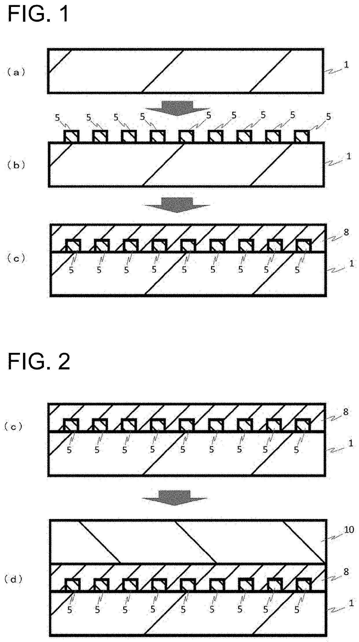
1. Fabrication of Stacked Structure

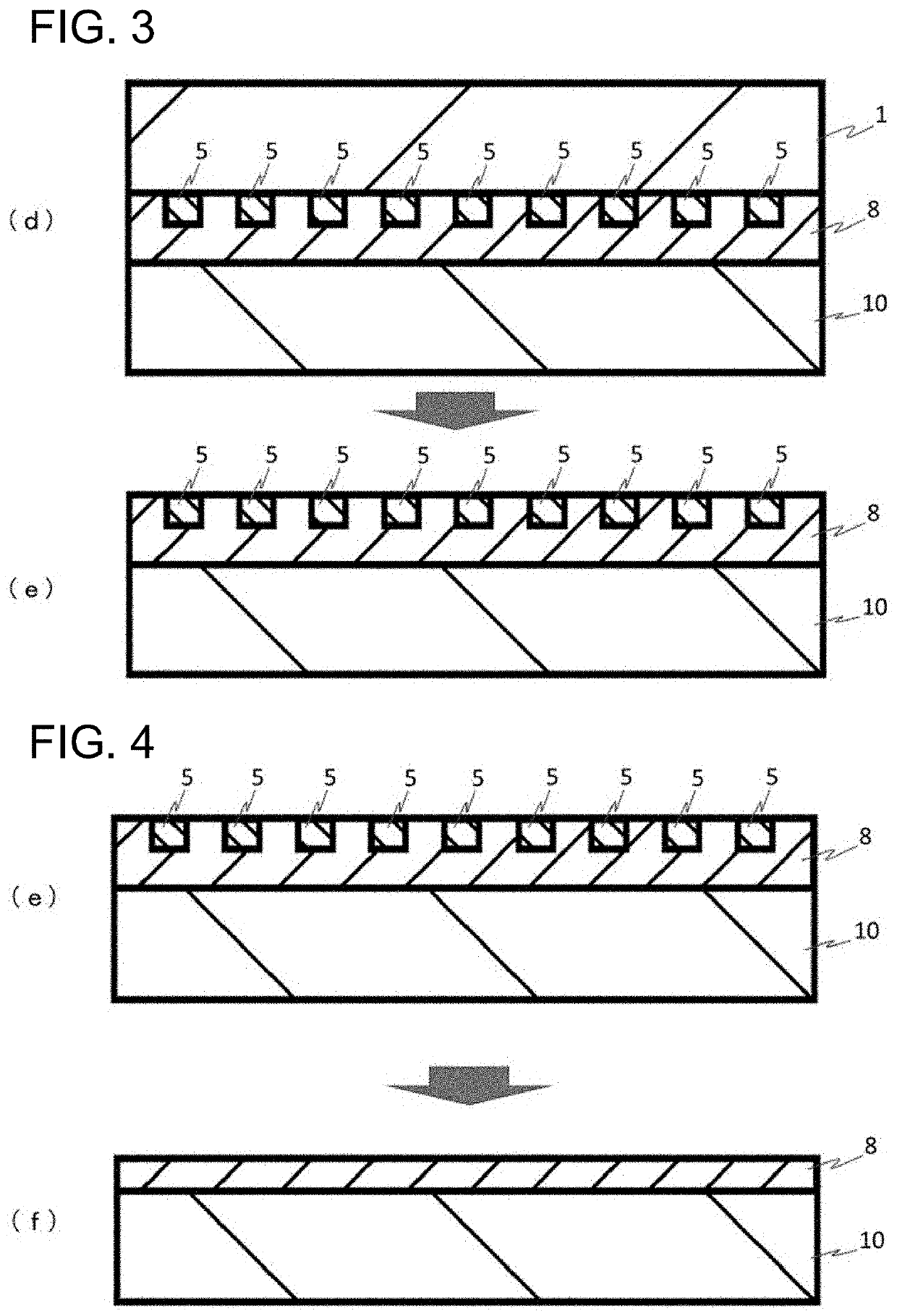
[0132]An ELO mask is formed on a front surface as a crystal growth substrate. It is to be noted that a sapphire substrate is used as the crystal growth substrate. In the present disclosure, it is preferable to use a sapphire substrate whose principal plane is an r plane or an S plane as the sapphire substrate. FIG. 1(a) shows a sapphire substrate 1. As shown in FIG. 1(b), an ELO mask 5 having a striped pattern is formed on a crystal growth surface of the sapphire substrate 1. A crystal growth layer of α-Ga2O3 is formed by mist CVD using the crystal growth substrate of FIG. 1(b), and a multilayer structure of FIG. 1(c) is obtained. The multilayer structure (c) has a crystal growth layer 8 formed on the sapphire substrate 1 with the ELO mask 5 on a front surface. After the multilayer structure (c) is obtained, a SiC substrate is adhered to the crystal growth layer 8 as a support substrate 10, and a multilayer structure of FIG. 2(d) is obtained. After...


PUM

PropertyMeasurementUnit
Lengthaaaaaaaaaa
Lengthaaaaaaaaaa
Lengthaaaaaaaaaa

Abstract

Provided is a laminated structure that has a crystalline film having a large area, which is useful for a semiconductor device, etc., and having a good film thickness distribution in which the film thickness is 30 μm or less, and that has excellent heat dissipation. In a laminated structure in which a crystal film containing a crystalline metal oxide as a main component is laminated on a support directly or with another layer therebetween, the support has a thermal conductivity of 100 W / m·K or more at room temperature, and the crystal film has a corundum structure. Furthermore, the film thickness of the crystal film is 1 μm to 30 μm, the area of the crystal film is 15 cm2 or more, the distribution of the film thickness in the area is in the range of ±10% or less.

Description

CROSS REFERENCE TO RELATED APPLICATION[0001]This application is a continuation-in-part application of International Patent Application No. PCT / JP2020 / 036990 (Filed on Sep. 9, 2020), which claims the benefit of priority from Japanese Patent Application Nos. 2019-179861 (filed on Sep. 30, 2019), 2019-179862 (filed on Sep. 30, 2019) and 2019-179863 (filed on Sep. 30, 2019).[0002]The entire contents of the above applications, which the present application is based on, are incorporated herein by reference.1. FIELD OF THE INVENTION[0003]The present disclosure relates to a multilayer structure that is useful for semiconductor devices, a semiconductor device, a semiconductor system, and a method of producing a multilayer structure.2. DESCRIPTION OF THE RELATED ART[0004]A semiconductor device using gallium oxide (Ga2O3) with a wide band gap is drawing attention as a next-generation switching element that can achieve high withstand voltage, low loss, and high heat resistance, and is expected ...

Claims


Application Information

Patent Timeline
IPC IPC(8): H01L29/04H01L29/12H01L21/02C30B29/16C30B25/18H01L29/49
CPCH01L29/04H01L29/12H01L29/4925C30B29/16C30B25/18H01L21/0242H01L29/24H01L23/3738H01L29/045H01L21/34H01L21/02565H01L21/6835H01L2221/6835C23C16/40C30B33/06H01L29/739H01L29/78H01L29/861H01L29/868H01L29/872C30B25/04H01L21/02647H01L21/02414H01L21/02433H01L21/02483H01L21/0262H01L21/02628H01L23/373H01L23/3736H01L23/4334H01L23/42H01L21/4871C03B33/06H01L29/772H01L21/20
Inventor OSHIMA, TAKAYOSHITORIYAMA, TATSUYA
Owner FLOSFIA
Why Eureka
Try Eureka