Mask, method of manufacturing the same, method of forming thin film pattern, method of manufacturing electro-optical device

A technology of thin film pattern and manufacturing method, which is applied in the direction of electric light source, lighting device, electroluminescent light source, etc., can solve the problems such as the inability to manufacture evaporation masks and the increase of error accumulation value, and achieve the purpose of suppressing the amount of etching and reducing The effect of thickness

Inactive Publication Date: 2005-09-28
SEIKO EPSON CORP
View PDF2 Cites 5 Cited by
  • Summary
  • Abstract
  • Description
  • Claims
  • Application Information

AI Technical Summary

Problems solved by technology

Therefore, once a large organic EL panel is manufactured with a metal mask, the error accumulation value caused by thermal expansion will increase, and the limit of using a metal mask can only manufacture small and medium-sized panels of 20 inches at best.
[0010] And for the evaporation mask that adopts silicon substrate described in above-mentioned patent document 2, also have the following problem: because silicon ingot diameter is 300 millimeters, so silicon substrate only has the size below 300 millimeters in diameter, can't manufacture and above screen Evaporation mask corresponding to the size

Method used


Image

  • Mask, method of manufacturing the same, method of forming thin film pattern, method of manufacturing electro-optical device
  • Mask, method of manufacturing the same, method of forming thin film pattern, method of manufacturing electro-optical device
  • Mask, method of manufacturing the same, method of forming thin film pattern, method of manufacturing electro-optical device

Examples


Embodiment Construction

[0083] A mask according to an embodiment of the present invention will be described below with reference to the drawings.

[0084] (manufacturing of masks)

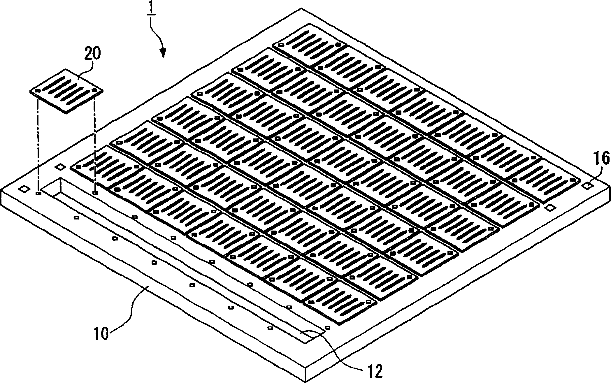
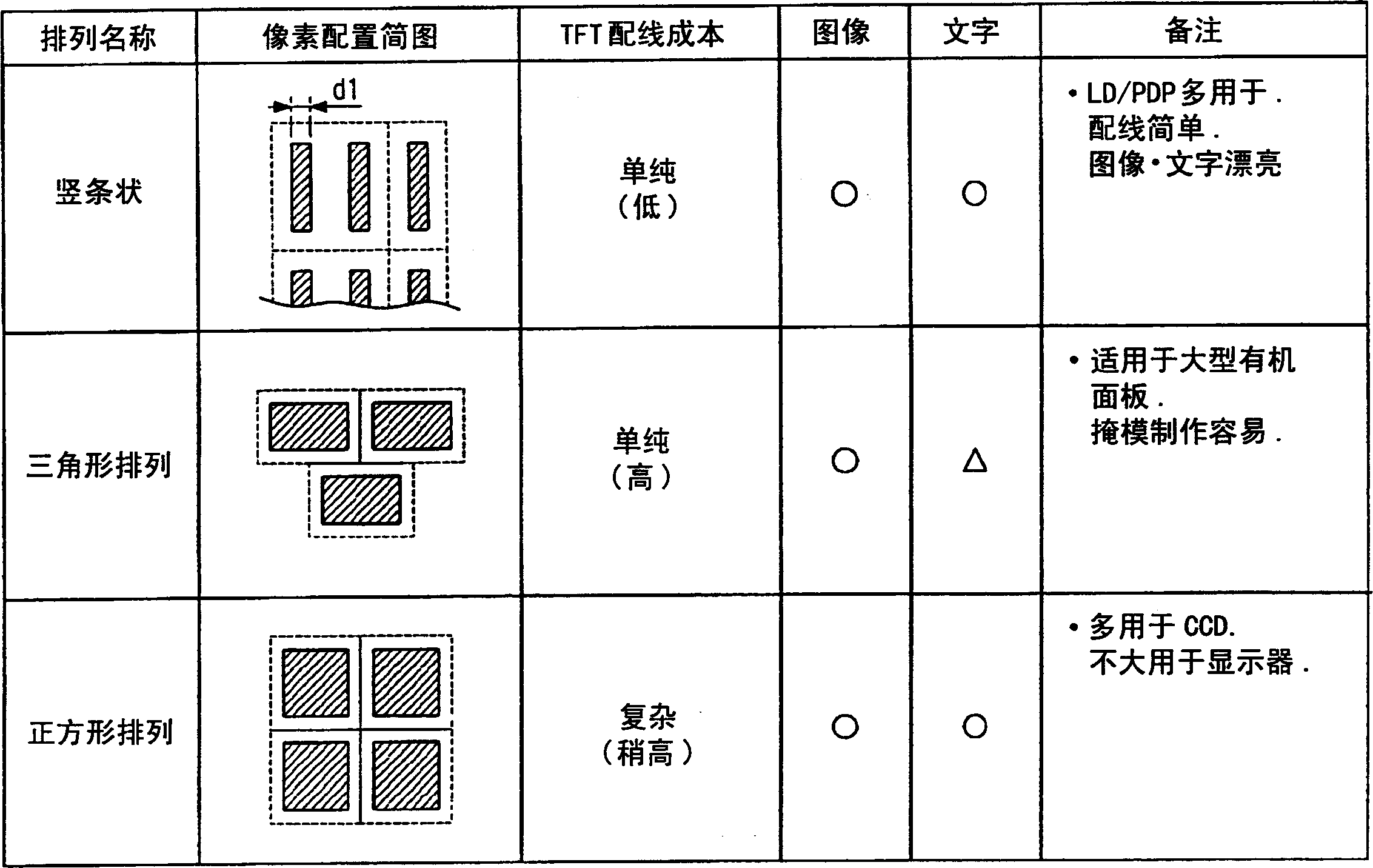
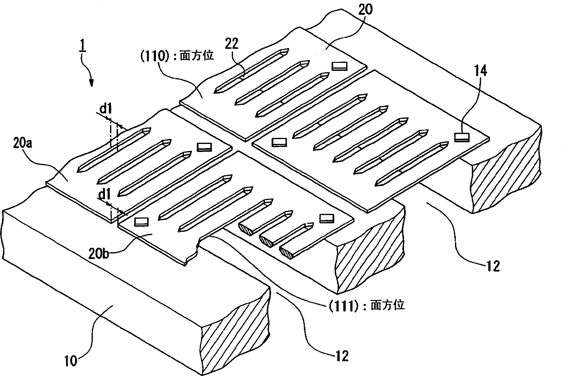
[0085] figure 1 It is a schematic perspective view which shows the mask which concerns on embodiment of this invention. figure 2 is used to express figure 1 Diagram of an example of a pixel pattern arrangement formed by the mask shown. image 3 Yes figure 1 An enlarged perspective view of the main part of the mask shown. The mask 1 of this embodiment can be used as a vapor deposition mask, for example.

[0086] The mask 1 has a configuration in which a plurality of chips 20 are mounted on a support substrate 10 as a base substrate. In this embodiment, the chip 20 is made of silicon. Moreover, the chip 20 can also be made of metal materials. Each chip 20 is arranged so as to be bonded to the substrate 10 . Further, mask alignment marks 16 are formed on the support substrate 10 . The mask alignment mark 16 is a m...


PUM

PropertyMeasurementUnit
diameteraaaaaaaaaa
thicknessaaaaaaaaaa

Abstract

The invention relates to providing a mask that can cope with increasing the size of a region on which a film to be formed and be patterned in high accuracy, a method of manufacturing the same, a method of forming a thin film pattern, a method of manufacturing an electro-optical device, and electronic equipment. A supporting substrate 10, and a plurality of chips 20 attached to the supporting substrate 10 are included. The chip 20 has an opening corresponding to at least a part of shape of a thin film pattern formed on a given surface. The area occupied by the chip 20 is smaller than an area of the thin film pattern using the plurality of chips 20.

Description

Technical field: [0001] The present invention relates to a mask, a method for manufacturing the mask, a method for forming a thin film pattern, a method for manufacturing an electro-optical device, and an electronic device. Background technique: [0002] An organic EL (electroluminescence) panel, which is one of electro-optical devices, is composed of a self-luminous display element having a laminated thin-film structure and a high-speed response. Therefore, such an organic EL panel can constitute a display device that is light and excellent in correspondence with animation, and has recently attracted much attention as a flat panel display (FPD) television. As a representative manufacturing method of an organic EL panel, it is disclosed in Applied Physics Communications, Vol. 51, No. 12, pp. 913-914 (1987). That is to say, use photolithography to pattern a transparent anode such as ITO (indium tin oxide) into a desired shape, and then use a vacuum evaporation device to form...

Claims


Application Information

Patent Timeline
Patent Type & Authority Applications(China)
IPC IPC(8): H05B33/10C23C14/04H01L23/544H01L51/50H01L51/56
CPCH01L23/544C23C14/042H01L2924/12044H01L2924/0002H01L2924/00H04M1/0237H04M1/23
Inventor 四谷真一桑原贵之池原忠好
Owner SEIKO EPSON CORP
Why Eureka
Try Eureka