

Laminate, method of manufacturing the same, and method of manufacturing electronic component
a technology of laminate and electronic components, which is applied in the direction of metal layered products, water-setting substance layered products, synthetic resin layered products, etc., can solve the problems of defective products, electronic components, and inability to easily remove gel from the substrate, and achieve excellent heat resistance, low elastic modulus, and low stress.
- Summary
- Abstract
- Description
- Claims
- Application Information
AI Technical Summary
Benefits of technology
Problems solved by technology
Method used
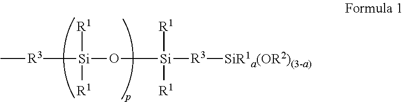
Image

Examples
examples
[0143]Hereinafter, the present invention will be described by way of examples, but the present invention is not limited thereto. In the examples shown below, the following compounds or compositions were used as raw materials.[0144]Component (A1-1): dimethylsiloxane polymer capped at both terminals with vinyldimethylsiloxy groups (polymerization degree of siloxane: about 540, vinyl group content: 0.13 weight %)[0145]Component (A1-2): dimethylsiloxane polymer capped at both terminals with vinyldimethylsiloxy groups (polymerization degree of siloxane: about 315, vinyl group content: 0.22 weight %)[0146]Component (A1-3): dimethylsiloxane / vinylmethylsiloxane copolymer capped at both terminals with trimethylsiloxy groups (polymerization degree of siloxane: about 1330, vinyl group content: about 0.47 weight %)[0147]Component (A2): resinous organopolysiloxane composed of trimethylsiloxy units (M units), vinyldimethylsiloxy units (MVi units), and Q units (vinyl group content: about 4.1 weigh...
PUM
| Property | Measurement | Unit |
|---|---|---|
| frequency | aaaaa | aaaaa |
| frequency | aaaaa | aaaaa |
| tan δ | aaaaa | aaaaa |
Abstract
Description
Claims
Application Information