Insulated metal substrate and method for manufacturing same

a technology of metal substrate and insulating metal, which is applied in the field of insulating metal substrate, can solve the problems of difficult mechanical engineering process brittle ceramic, and difficult thermal management of dbc ceramic substrate,

Active Publication Date: 2022-08-25
POLYTRONICS TECH
View PDF4 Cites 0 Cited by
  • Summary
  • Abstract
  • Description
  • Claims
  • Application Information

AI Technical Summary

Benefits of technology

[0008]To solve aforementioned problems, the present invention provides an insulated metal substrate (IMS) and a method for manufacturing the same. The layers in the IMS do no separate from each other, and the misalignment problem can be avoided. The IMS of the present invention has excellent heat conductivity and high glass transition temperature Tg, thus being particularly suitable for high power applications that requires thick copper layer.
[0042]According to the present invention, an insulated metal substrate (IMS) and a method for manufacturing the same are disclosed. The present invention can avoid the misalignment problem, and there is no issue of layer delamination. In addition, the IMS has excellent heat conductivity and high glass transition temperature Tg. Accordingly, the present invention is particularly suitable for high power applications, thus providing a solution to the traditional IMS which encounters the problems as described above.

Problems solved by technology

Although DBC ceramic substrate can endure temperature as high as over 1000° C., ceramic is brittle and fragile, it is difficult for DBC ceramic substrate to undergo mechanical engineering process such as drilling and / or cutting process during manufacturing process thereof.
Thus, recently, thermal management becomes a thorny problem.
However, as said above, DBC ceramic substrate have problems of delamination at high temperature and difficulty in mechanical engineering process.
However, according to this method, these electrically conductive metal blocks cannot be accurately disposed on the insulation layer, thus resulting in misalignment problem.
Such structure design makes the hot presser, during the hot-pressing step, cannot apply a uniform pressure on entire upper surface of the heat dissipation fin.
As a result, after hot-pressing is completed, bonding strength between layers of IMS is poor.
In particular, if IMS is used in extremely poor environment like high temperature and high humidity conditions, occurrence of separation or peeling between layers is common, and this cause serious issue.

Method used


Image

  • Insulated metal substrate and method for manufacturing same
  • Insulated metal substrate and method for manufacturing same
  • Insulated metal substrate and method for manufacturing same

Examples


Embodiment Construction

[0048]The making and using of the presently preferred illustrative embodiments are discussed in detail below. It should be appreciated, however, that the present application provides many applicable inventive concepts that can be embodied in a wide variety of specific contexts. The specific illustrative embodiments discussed are merely illustrative of specific ways to make and use the invention, and do not limit the scope of the invention.

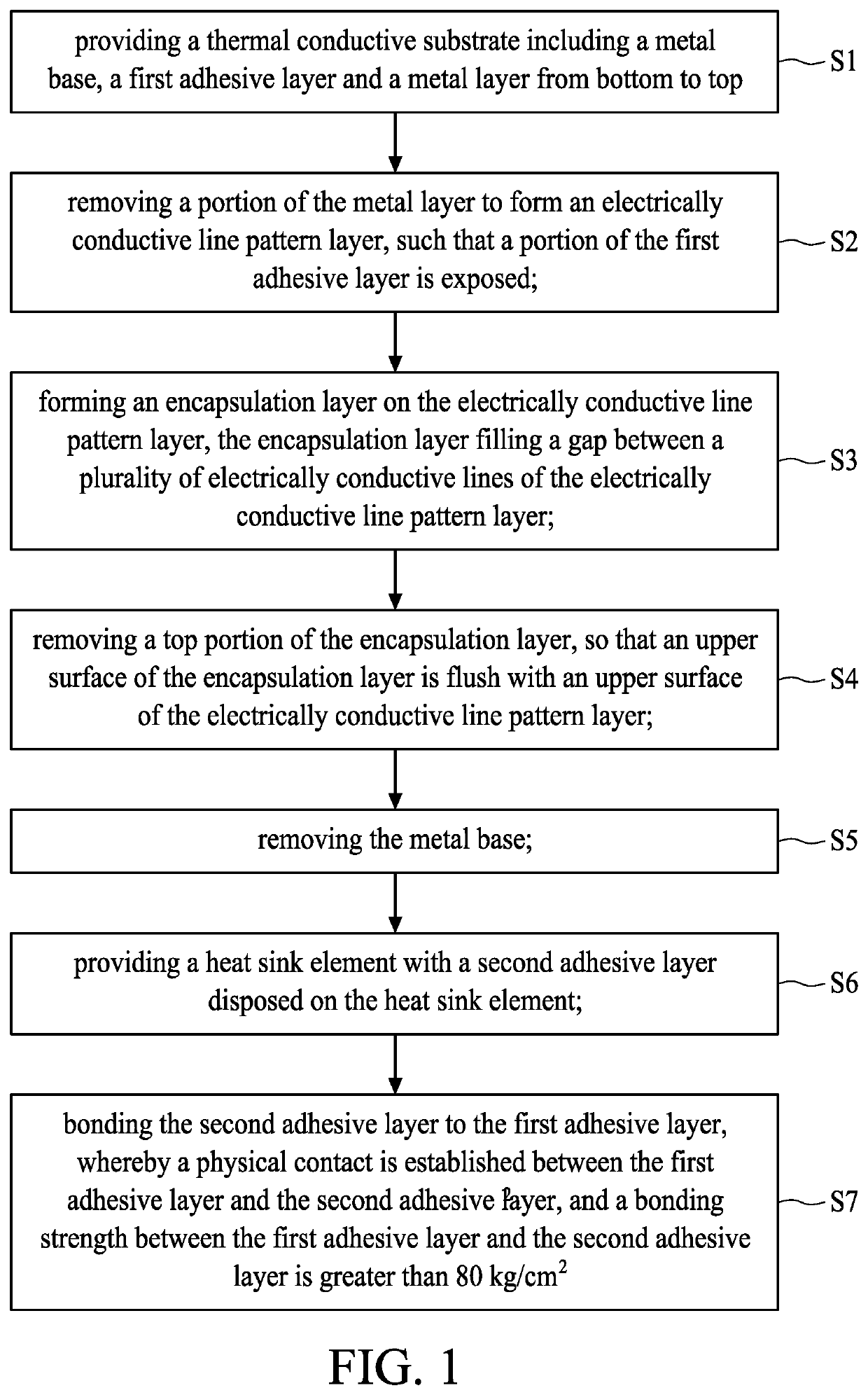
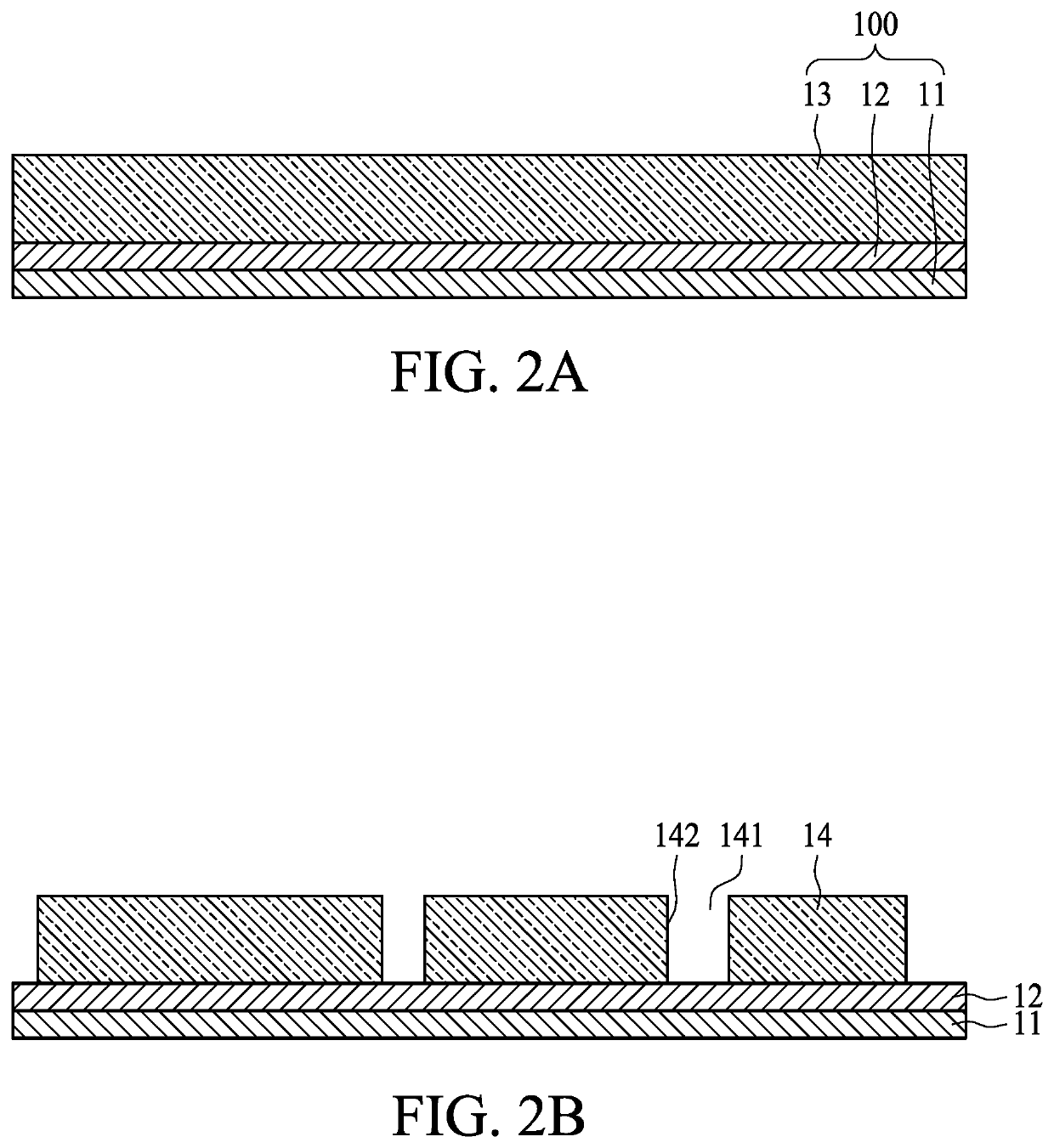
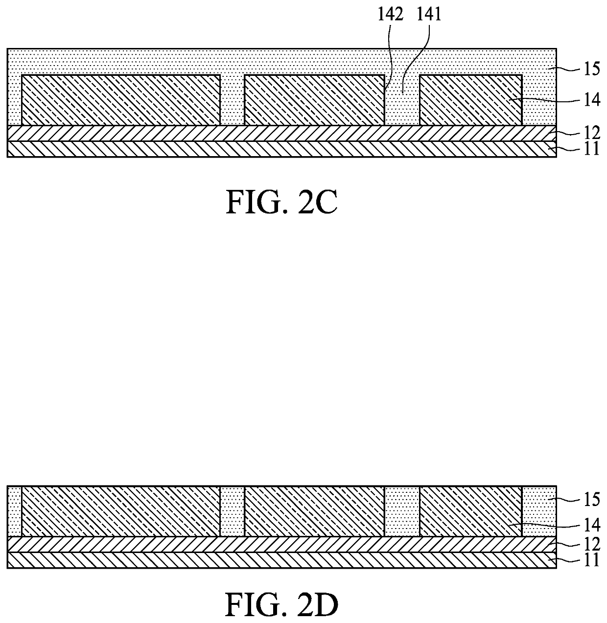
[0049]FIG. 1 shows a flowchart of a method for manufacturing an IMS in accordance with an embodiment of the present invention. The method includes the following steps. In step S1, a thermal conductive substrate is provided, which includes a metal base, a first adhesive layer and a metal layer from bottom to top. In step S2, a portion of the metal layer is removed to form an electrically conductive line pattern layer, such that a portion of the first adhesive layer is exposed. In step S3, an encapsulation layer is formed on the electrically conducti...


PUM

PropertyMeasurementUnit
thicknessaaaaaaaaaa
temperatureaaaaaaaaaa
glass transition temperature Tgaaaaaaaaaa

Abstract

An insulated metal substrate (IMS) and a method for manufacturing the same are disclosed. The IMS includes an electrically conductive line pattern layer, an encapsulation layer, a first adhesive layer, a second adhesive layer, and a heat sink element. The encapsulation layer fills a gap between a plurality of electrically conductive lines of the electrically conductive line pattern layer. An upper surface of the encapsulation layer is flush with an upper surface of the electrically conductive line pattern layer. The first and second adhesive layer are disposed between the electrically conductive line pattern layer and the heat sink element. A bonding strength between the first adhesive layer and the second adhesive layer is greater than 80 kg / cm2.

Description

BACKGROUND OF THE INVENTION(1) Field of the Invention[0001]The present application relates to an insulated metal substrate, and more specifically, to an insulated metal substrate suitable for high power applications.(2) Description of the Related Art[0002]Generally, a commonly used thermal conductive board could be an insulated metal substrate (IMS) or a directed bonded copper (DBC) ceramic substrate. An electronic device, such as an integrated circuit (IC) chip, could be built on the thermal conductive board and is electrically coupled thereto to establish electrical connection therebetween. In operation, the electronic device generates heat which gradually accumulates on the device as time goes on. Heat could be either dissipated upwards via a metal conductive line pattern on surface of the board towards the above ambient environment, or dissipated downwards from the thermal conductive board to the below space. In other words, the thermal conductive board serves as a heat dissipat...

Claims


Application Information

Patent Timeline
Patent Type & Authority Applications(United States)
IPC IPC(8): H01L23/373B32B7/12B32B15/092B32B15/20H01L23/14H01L21/48
CPCH01L23/3735B32B7/12B32B15/092B32B15/20H01L23/142H01L21/4807B32B2457/04B32B2457/08H01L23/145H05K1/0204H05K1/02H01L23/3737H01L23/36H05K3/44H05K3/202H05K2201/0376H05K1/056B32B2264/102B32B2307/302H01L21/31051B32B2037/243B32B2307/102B32B2311/00B32B2037/1253B32B38/10B32B38/1833B32B2309/105B32B2309/02
Inventor YU, FENG-CHUNLO, KAI-WEILEE, WEN FENGCAI, RU-YI
Owner POLYTRONICS TECH
Why Eureka
Try Eureka