Buried heterostructure with aluminum-free active layer and method of making same

a heterostructure and active layer technology, applied in semiconductor devices, lasers, semiconductor lasers, etc., can solve the problem of providing a structure having a sufficiently good temperature dependen

Inactive Publication Date: 2000-01-04
TELEFON AB LM ERICSSON (PUBL)
View PDF15 Cites 31 Cited by
  • Summary
  • Abstract
  • Description
  • Claims
  • Application Information

AI Technical Summary

Problems solved by technology

However, none of the above mentioned disclosures provides a

Method used


Image

  • Buried heterostructure with aluminum-free active layer and method of making same
  • Buried heterostructure with aluminum-free active layer and method of making same
  • Buried heterostructure with aluminum-free active layer and method of making same

Examples


Embodiment Construction

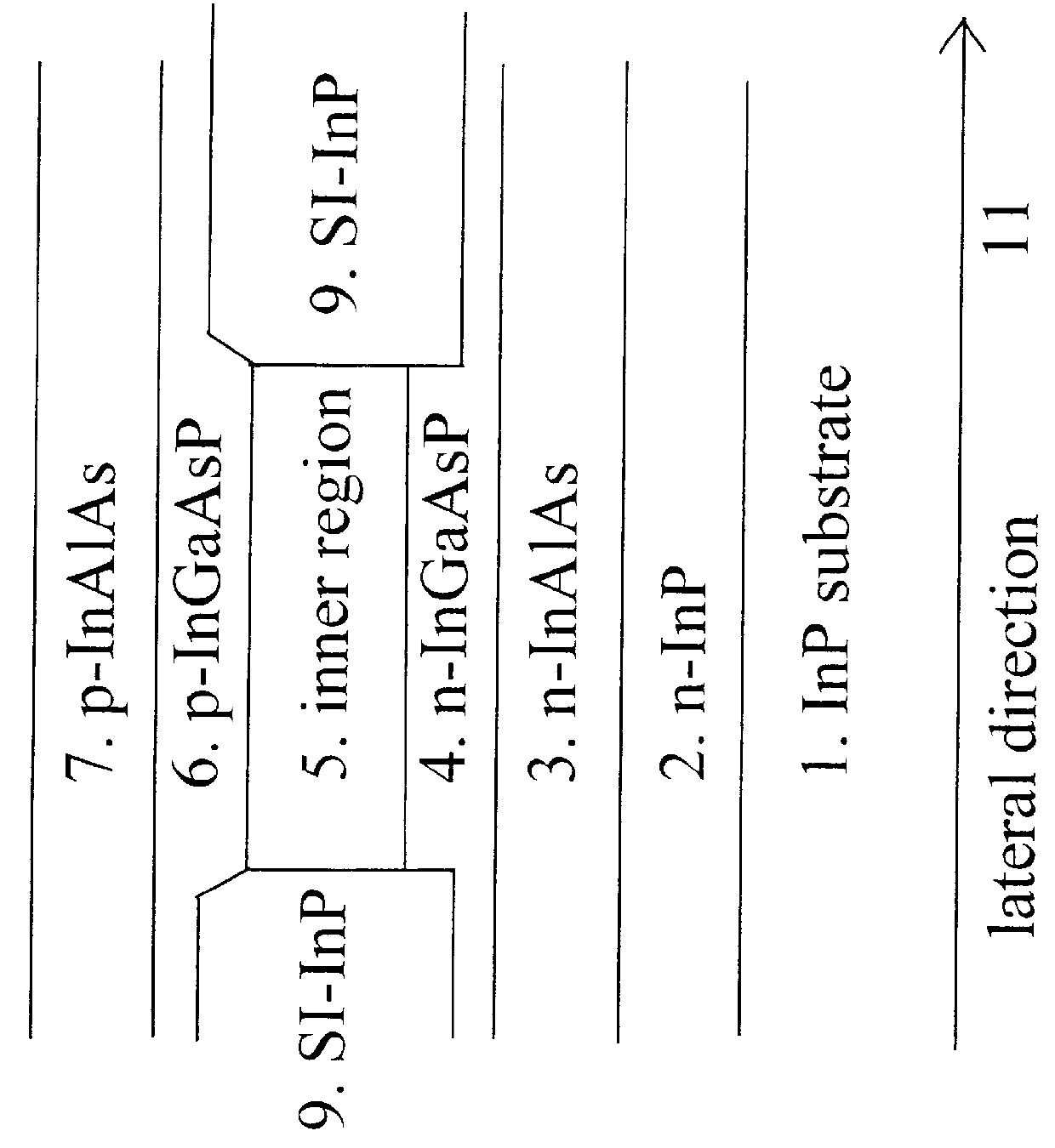
In FIG. 1 a buried heterostructure is shown in a schematic view and it is based on InP and is similar to that illustrated in FIGS. 2 and 3 of the patent U.S. Pat. No. 5,381,434 cited above. The structure can be produced by executing the following process steps:

On some substrate 1, such as a InP substrate, an n-doped InP layer 2 is epitaxially grown. On this n-doped InP layer 2 an n-doped aluminium containing layer 3 such as an InAlAs layer is epitaxially grown and on this an n-doped InGaAsP layer 4 is grown. On this InGaAsP layer 4 the inner region 5 for which the confinement of the photons and electrons is intended is grown. On top of this inner region 5 a p-doped InGaAsP layer 6 is grown.

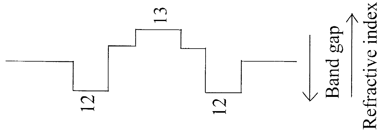
Different structures can be provided for the inner region 5: it can be a passive waveguide, i.e. have a band gap of energy higher than the signal photons, intended for a tuning region and it would then also contain a grating layer, it can be an active waveguide for laser or laser amplifier operati...


PUM


Abstract

An epitaxially grown semiconductor heterostructure has an inner region (5) which is substantially laterally confined by confinement regions (9) and has enhanced transverse confinement by enhanced transverse confinement layers (3, 7). The latter layers are not exposed outside the growth chamber during processing, by stopping the etching for producing the lateral confinement, above the lower enhanced transverse confinement layer (3) and growing such an upper layer (7) after making the lateral confinement regions (9). The structure is intended to be used in particular having the inner region act as an active laser region, for instance in InP-based 1.3 mu m wavelength lasers. Then the simultaneous lateral confinement, enhanced transverse confinement and exposure protection enables simultaneously a low threshold current, a small temperature sensitivity and reliable, long life operation. The enhanced transverse confinement layers (3, 7) could comprise aluminium protected from oxidation during processing. Such a laser will then be protected from a declined reliability.

Description

The present invention relates to a structure for carrier confinement, in particular for InP-based lasers and other optoelectronic devices.InP-based 1.3 .mu.m wavelength lasers which operate at high temperatures and are intended for low threshold and / or low bias current operation are believed to play an important role as transmitters in future access networks, see S. Yamashita et al. "Low-threshold (3.2 mA per element) 1.3 .mu.m InGaAsP MQW laser array on a p-type substrate", IEEE Photonics Technology Letters, vol. 4, No. 9, pp. 954-957, 1992 and H. Nobuhara et al. "1.3 .mu.m wavelength, low-threshold strained quantum well laser on p-type substrate", Electronic Letters, vol. 30, No. 16, pp. 1292-1293, 1994.Due to the expected high temperatures it is crucial to improve their poor temperature dependence, which is believed to be partly caused by poor carrier confinement or carrier leakage in the growth, transverse direction, see P. A. Andrekson et al. "Effect of thermionic electron emis...

Claims


Application Information

Patent Timeline
IPC IPC(8): H01S5/227H01S5/00H01S5/32H01S5/343H01S5/20H01S5/183H01S5/22H01S5/34
CPCB82Y20/00H01S5/2275H01S5/18308H01S5/2205H01S5/2224H01S5/3211H01S5/34306H01S5/3434H01S2301/173H01S5/30
Inventor OHLANDER, ULFRASK, MICHAELSTOLTZ, BJORN
Owner TELEFON AB LM ERICSSON (PUBL)
Why Eureka
Try Eureka