
Enhanced reactive DC sputtering system

a sputtering system and reactive technology, applied in the field of reactive sputtering systems, can solve the problems of electrical discharge or arc, electrical breakdown of the insulator, and special coating process type, etc., to achieve enhanced processing, dissipate any charge build-up, and enhance processing

Inactive Publication Date: 2000-02-15
ADVANCED ENERGY IND INC
View PDF7 Cites 118 Cited by
  • Summary
  • Abstract
  • Description
  • Claims
  • Application Information

AI Technical Summary

Benefits of technology

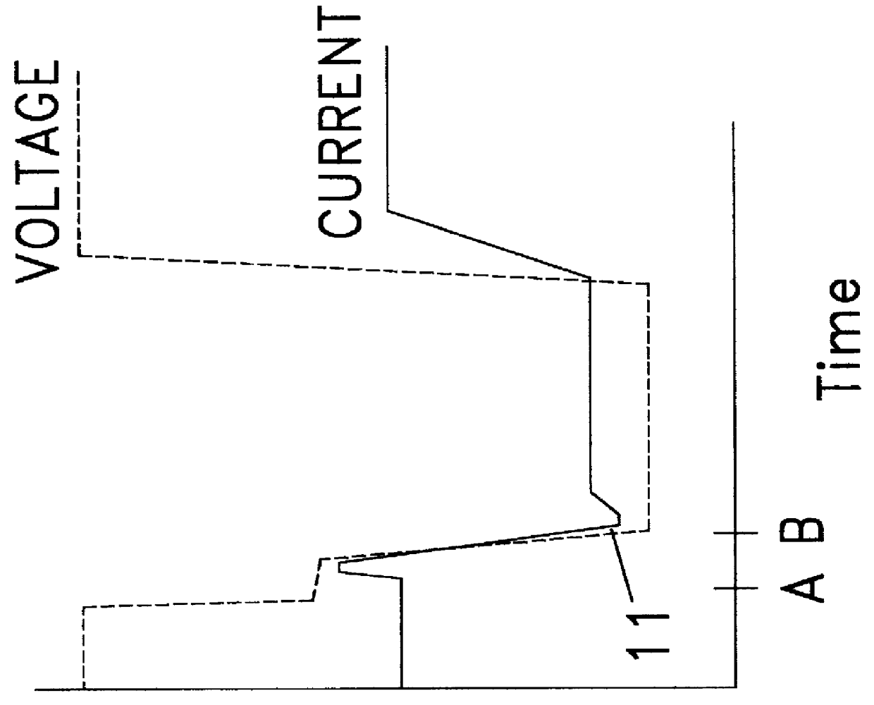
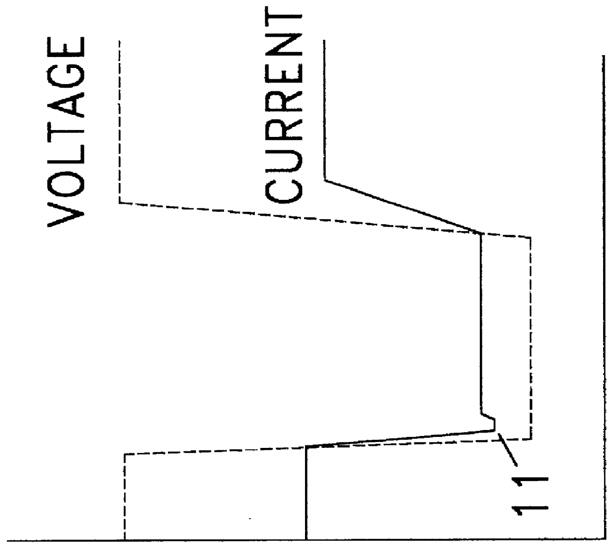
The present invention discloses both the fundamental understandings and circuitry designs which virtually eliminate the occurrences of arcs and which afford processing advantages within a reactive DC sputtering system. In one regard, the present invention discloses a technique of periodically refurbishing the plasma and the electrical state of surfaces in the deposition system so as to avoid potential arcing conditions in the first place. In another regard, it discloses a technique of processing in a different manner which enhances processing. In addition the invention encompasses a variety of embodiments through which the supply of direct current power may be interrupted, through which the plasma current may be immediately stopped or decreased upon the actual or incipient occurrence of an arc, through which the voltage may be reversed, and through which the condition giving rise to the potential arc in the first place is negated. In its preferred embodiment, the invention involves a two stage, tapped inductor which is switched to ground. Periodically or upon the occurrence of an arc condition (an actual or incipient occurrence of an arc) the switch is activated and the circuitry acts to reverse the voltage applied to the plasma. This may either enhance processing in general or may affirmatively attract electrons from the plasma to dissipate any charge build-up which may give rise to an arcing situation. The invention also discloses techniques for sensing an arc condition or even the incipient occurrence of an arc so that immediate response is possible.
Accordingly it is an object of the invention to periodically refurbish the plasma and the electrical state of the system surfaces within a DC plasma processing system to substantially reduce the probability of an arc occurring. A goal is to achieve this automatically and perhaps even regularly. Further, a goal is not just to react to arcs which are occurring (or just about to occur), but to avoid such occurrences in the first place. Thus a goal is to present general design criteria through which systems can be manipulated to minimize or even avoid arc occurrences in the first place by periodically refurbishing the plasma and discharging system surfaces of ion buildup.
It is a further object of the invention to avoid the undesirable effects of any arcs which do occur. In so doing, the invention has a goal of efficiently reacting to arcs in a manner which minimizes any energy impact of the arc upon the coating process. As part of avoiding undesirable effects on the overall plasma processing system, the invention has a goal of acting in a manner which avoids any quenching of the plasma. This not only minimizes the effects of the arc, but it also allows restoration of the process with minimum delay. In proposing an efficient design, the present invention has as a further goal to provide a technique which may be easily adapted to existing power supply and plasma processing system designs. It also is disclosed in a fashion of an improved power supply design which is independent of the system and thus may be utilized in other similar applications.

Problems solved by technology

One of the challenges in many such applications is that electrical discharges or arcs can occur.
As one example, this type of coating process is particularly challenging because it involves forming insulating regions on the material target and bombarding them with ions.
This leads to charging of the insulating regions which can cause electrical breakdown of the insulator.
These arc discharges are undesirable not only because they represent potential non-uniformities in the coating process, but also because they can lead to the creation of particulates which can in turn create defects in sensitive items such as computer disks and integrated circuits.
Also, it may be necessary to protect the power supply from arc discharges by turning it off momentarily, and this can adversely affect throughput.
Similarly, the processing itself can be adversely affected by such insulating regions.
Often these effects, and their solutions, are unpredictable and are achieved after some trial and error without a complete understanding of the exact impact on the process.
With respect to the observable problem of arc occurrences, this aspect has been well known to those skilled in the art, and has been addressed with limited success in ordinary metallic sputtering and reactive sputtering of films that are not too insulating.
Unfortunately, most such solutions acted only after damage had been done and thus served to minimize, but not completely avoid, problems in more sensitive processing environments.
In spite of the fact that they inherently store less power and thus can be manipulated to minimize the negative effects of such arc occurrences, their use alone has not been sufficient for many processing environments.
This may have lead to duplication of efforts and limited progress in understanding the nature of the problem; as a result the development of solutions has primarily been the result of individual effort, rather than a coordinated approach.
Unfortunately this solution acts to increase the current in the arc initially and thus can intensify the problem before solving it.
Again, this solution is undesirable especially in refined processing environments, and none of the above solutions work adequately well when the process is reactive and the reaction product is a good insulator.
For this situation dc-powered reactive sputtering has generally been abandoned in favor of other, more expensive approaches (such as radio-frequency sputtering) because of the lack of a suitable arc-handling solution.

Method used


Image

  • Enhanced reactive DC sputtering system
  • Enhanced reactive DC sputtering system
  • Enhanced reactive DC sputtering system

Examples


Embodiment Construction

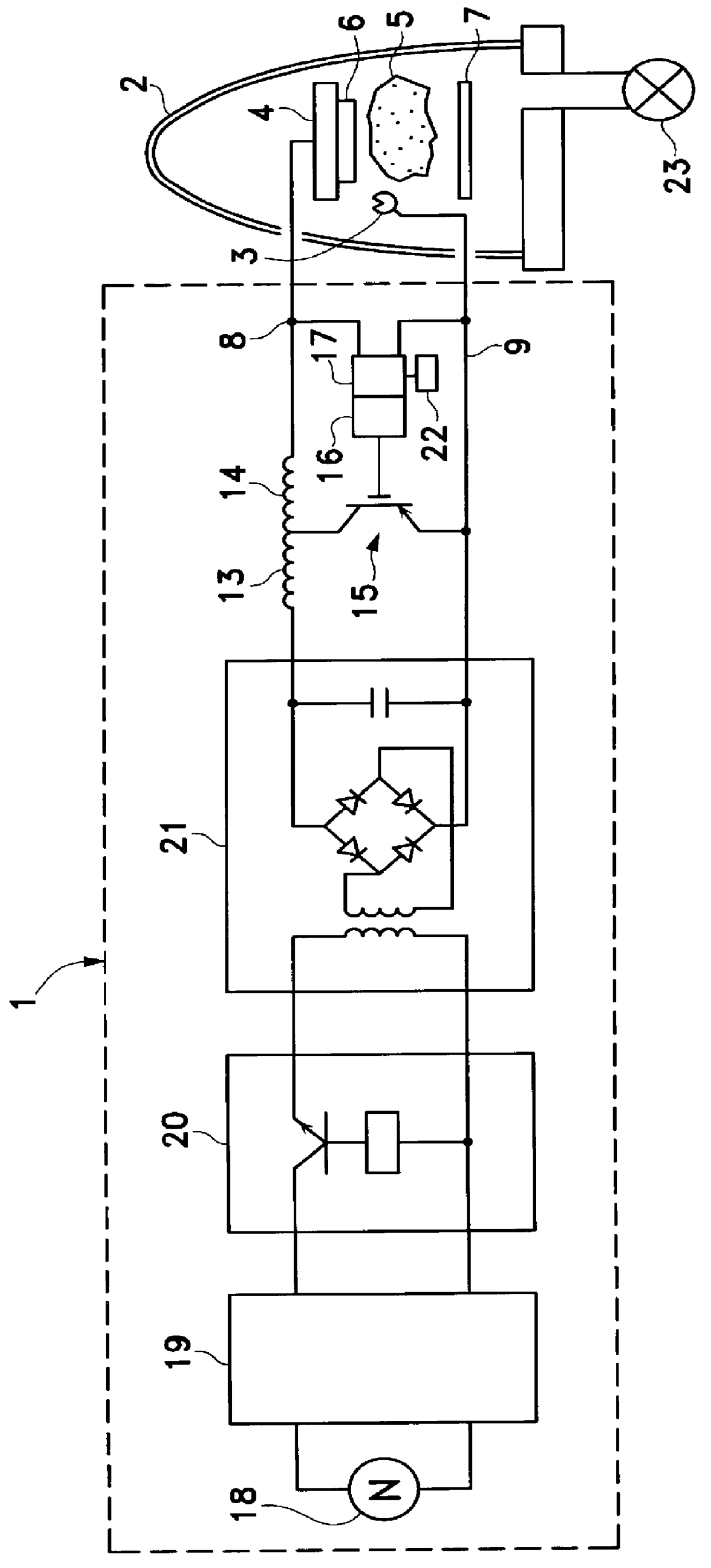
As will be readily understood, the basic concepts of the present invention may be embodied in a variety of ways. Referring to FIG. 1, the tapped inductor embodiment can be readily understood. In general, the reactive DC sputtering system includes the elements shown in FIG. 1. Specifically, DC power source (1) is connected to coating chamber (2) within which cathode (4) and anode (3) are contained. In the deposition mode, the DC power source (1) causes deposition of a coating material by creating an electric potential across material target (6) (or cathode (4)) and anode (3) to result in plasma (5). Plasma (5) then acts upon material target (6) so as to result in a coating on substrate (7). The material target (6) may be positioned or disposed so as to expose coating material which is consumed in the processing. As shown, such coating material may be the actual material of which the material target (6) itself is made through merely exposing one surface of material target (6). This co...


PUM

PropertyMeasurementUnit
Fractionaaaaaaaaaa
Fractionaaaaaaaaaa
Fractionaaaaaaaaaa

Abstract

An enhanced reactive plasma processing method and system useful for deposition of highly insulating films. A variety of alternative embodiments are allowed for varying applications. In one embodiment, a tapped inductor is switched to ground or some common level to achieve substantial voltage reversal of about 10% upon detection of an arc condition. This reversal of voltage is maintained long enough to either afford processing advantages or to allow restoration of uniform charge density within the plasma prior to restoration of the initial driving condition. A technique for preventing arc discharges involving periodically either interrupting the supply of power or reversing voltage is effected through a timer system in the power source.

Description

I. BACKGROUND OF THE INVENTIONThis invention generally relates to reactive sputtering systems in which a plasma effects some processing on a substrate. Specifically, the invention has application to DC sputtering when coating with some insulating materials formed by chemical reaction in the coating process. It also involves power supply designs used in such applications.The field of DC plasma processing is one which is well known. In these processes, a DC power supply creates an electric potential between a cathode and anode and thereby creates a plasma. In the deposition mode, the plasma then acts upon a material target to create a thin film on some substrate. This thin film may either be comprised of the target material itself or may be the result of some reaction with some element within the coating chamber. It is the latter case, called "reactive sputtering" with which the present invention is most concerned. Naturally both the materials and elements involved and the specific ap...

Claims


Application Information

Patent Timeline
IPC IPC(8): C23C14/34B01J19/08C23C16/50C23C14/38C23C16/509H01J37/34H01L21/31H05H1/00H05H1/24H05H1/46H05H1/48
CPCH01J37/34H01J2237/0206H01J2237/0044
Inventor DRUMMOND, GEOFFREY N.SCHOLL, RICHARD A.
Owner ADVANCED ENERGY IND INC
Learn More