Semiconductor device with stabilized junction
- Summary
- Abstract
- Description
- Claims
- Application Information
AI Technical Summary
Problems solved by technology
Method used
Image

Examples
example 2
(Hg,Cd)Te and (Zn,Hg)Te samples were polished chemomechanically, using 5% (v / v) solution of Br.sub.2 / ethylene glycol solution. Subsequently, within a time less than 5 min, 40 nm thick and 50 .mu.m diameter Ag spots were evaporated on their front surface. A large area C-paste back contact was applied to the opposite side of the sample.
The scheme of experiment was as described in example b) of the above description, b) Electromigration of silver into n-type MCT. Quantitatively all samples show the same behavior, which is identical to that described in example b.
Application of positive bias V.sub.inject.sup.n for time T.sub.disapp.sup.n to the silver spots results in formation of inhomeogeneously doped p-type area in the vicinity of the spot. This can be detected by measuring the Seebeck coefficient and by EBIC. Then the system evolves by itself into an n-p-n structure during a time T.sub.evolv.sup.n. The n-p-n structures that are formed in this way are stable in time.
TABLE 2 ________...
example 3
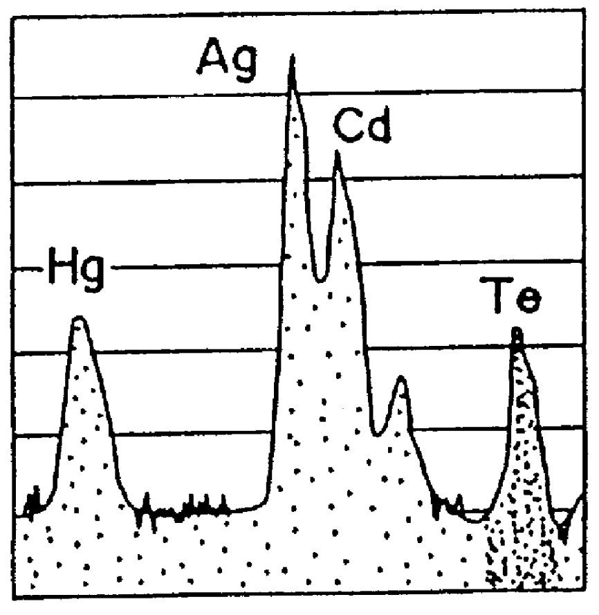
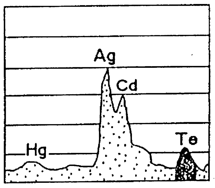
n-Hg.sub.0.3 Cd.sub.0.7 Te with n=3*10.sup.15, .mu.=400 cm.sup.2 (V*sec) was etched by Bromine Ethylene glycol solution (5 % v / v). A silver layer 1-4 .mu.m was evaporated on their surface. The sample was baked in vacuum (.ltoreq.2*10.sup.-5 mTorr) at 160.degree. C. for 24 h. After baking the edges of the samples were removed. The sample was cut to expose a surface perpendicular to the p-n junction, which was then polished. Electrical contact to the n and p parts of the samples was made by sputtering Au (contact resistance; 2*10.sup.2 +2*10.sup.3 .OMEGA. / mm). Originally the I-V characteristics are those of a diode. Current under reverse bias 4 V is about 0.1 .mu.A. EBIC line scans of cross section and I-V curves of a crystal of n-Hg.sub.0.3 Cd.sub.7 te, with n=3.multidot.10.sup.15 cm.sup.-3 and .mu.=400 cm.sup.2 / V.multidot.sec are shown in FIGS. 10a and 10b. The p-n junction is formed some 45 .mu.m inside the crystal by heating the sample with Ag for 24 hr at 160.degree. C. Then p-n...
example 4
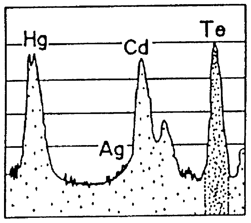
n-Hg.sub.0.3 Cd.sub.0.7 Te with n-3*10.sup.15, .mu.=400 cm.sup.2 / (V*sec) was etched by Bromine Ethylene glycol solution (5% v / v). A silver layer 1-4 .mu.m was evaporated on the surface. The sample was baked in vacuum (.ltoreq.2*10.sup.-5 mTorr) at 350.degree. C. for 8 h. After baking, the edges of the samples were removed. The sample was cut to expose a surface perpendicular to the p-n junction, which was then polished. Electrical contact to the n and p parts of the samples was made by sputtering Au (contact resistance: 2*10.sup.2 -2*10.sup.3 .OMEGA. / mm.sup.2).
Moderate heating to 180.degree. C. for 8 min. was applied to the sample containing a junction, located at 350 .mu.m depth (formed according to the description given in the previous paragraph). Then the junction was kept at room temperature.
FIGS. 12a, b, c show EBIC line scans of cross section of a crystal of n-(Hg.sub.0.3 Cd.sub.0.7) Te, with n=3.multidot.10.sup.15 cm.sup.-3 and .mu.=400 cm.sup.2 / V.multidot.sec, containing a...
PUM
 Abstract
Description
Claims
Application Information
 - R&D
- Intellectual Property
- Life Sciences
- Materials
- Tech Scout
- Unparalleled Data Quality
- Higher Quality Content
- 60% Fewer Hallucinations
Browse by: Latest US Patents, China's latest patents, Technical Efficacy Thesaurus, Application Domain, Technology Topic, Popular Technical Reports.
© 2025 PatSnap. All rights reserved.Legal|Privacy policy|Modern Slavery Act Transparency Statement|Sitemap|About US| Contact US: help@patsnap.com