Method for quantifying ultra-thin dielectric reliability: time dependent dielectric wear-out

Inactive Publication Date: 2000-04-04
ADVANCED MICRO DEVICES INC
View PDF4 Cites 38 Cited by
  • Summary
  • Abstract
  • Description
  • Claims
  • Application Information

AI Technical Summary

Problems solved by technology

The reliability of ultra-thin dielectric affects the overall reliability of microelectronic circuits.
In the first stage, the ultra-thin dielectric is damaged by injecting electrons under a high field bias.
During the second stage, the dielectric is subjected to a substantial tunneling conduction current that usually results in thermal breakdown due to the heating effects of the current flow.
Although t.sub.bd distributions may be constructed by observing these processes, at best the life-cycle approximation is subject to error as conventional dielectrics are subjected to dynamic stress over their useful lives just as microelectronic devices experience a time-varying bias during ordinary use.
However, the voltage-ramp test process fails to account for the dynamic stress dielectrics are subjected to as variations in electric fields may be random and do not normally occur in linear patterns.
Moreover, the voltage-ramp test common

Method used


Image

  • Method for quantifying ultra-thin dielectric reliability: time dependent dielectric wear-out
  • Method for quantifying ultra-thin dielectric reliability: time dependent dielectric wear-out
  • Method for quantifying ultra-thin dielectric reliability: time dependent dielectric wear-out

Examples


Embodiment Construction

In the drawings, depicted elements are not necessarily drawn to scale and alike and similar elements may be designated by the same reference numeral through several views.

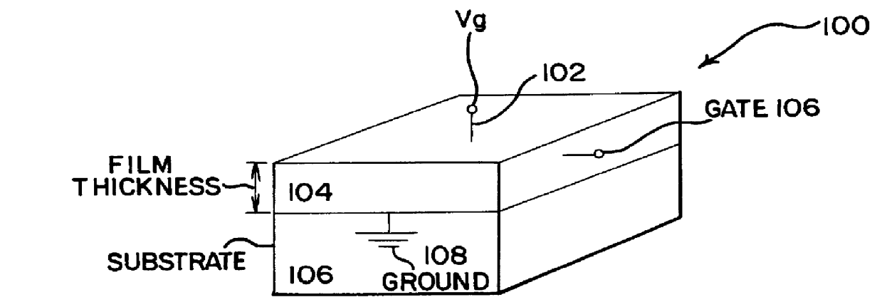
FIG. 1. shows a cross sectional view of an ultra-thin dielectric in accordance with a first embodiment of the invention. As shown, an electrode 102 is disposed on a planar surface area of an ultra-thin film oxide 104, which in turn is disposed on a semiconductor substrate 106 coupled to an electrical ground 108. A gate electrode 106 is disposed on a gate surface of the ultra-thin film oxide. Because good ohmic contact should be achieved through out an electrical field cycling, the selection of the electrode material will depend on the ultra-thin dielectric characteristics.

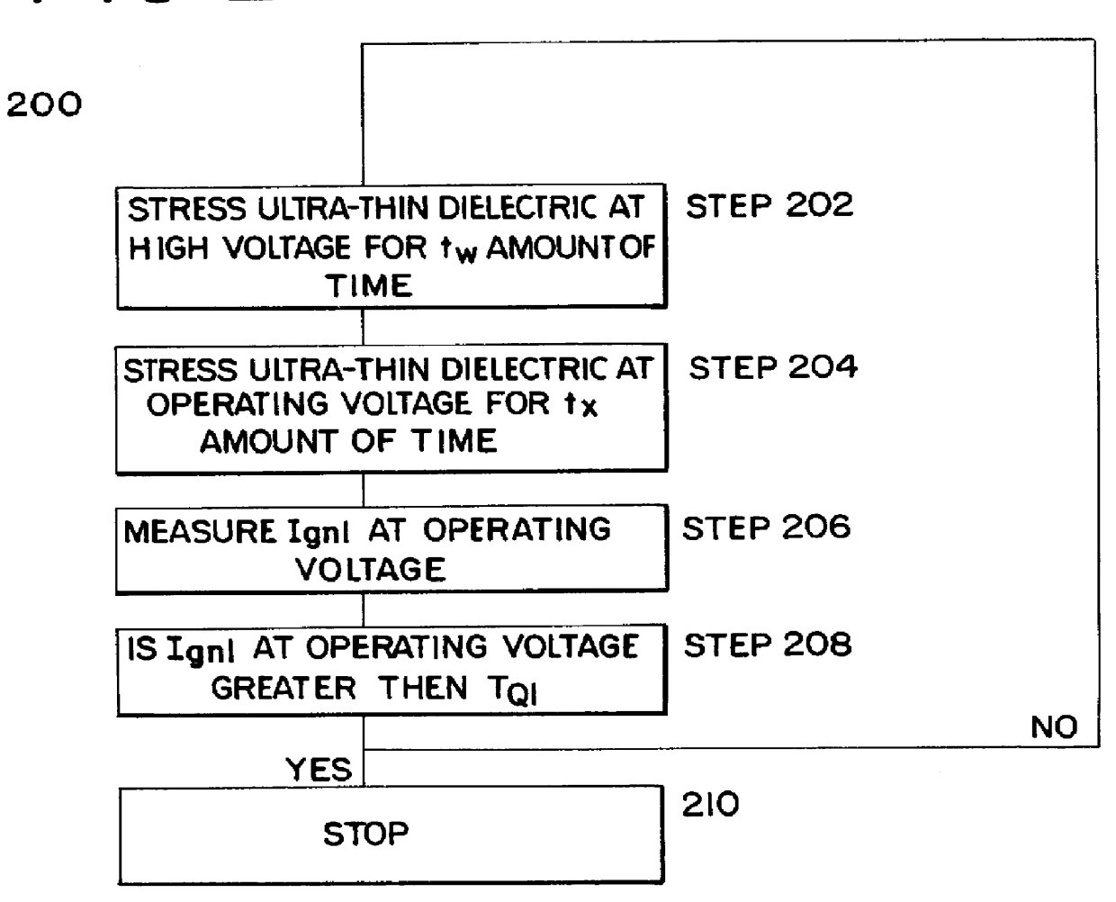
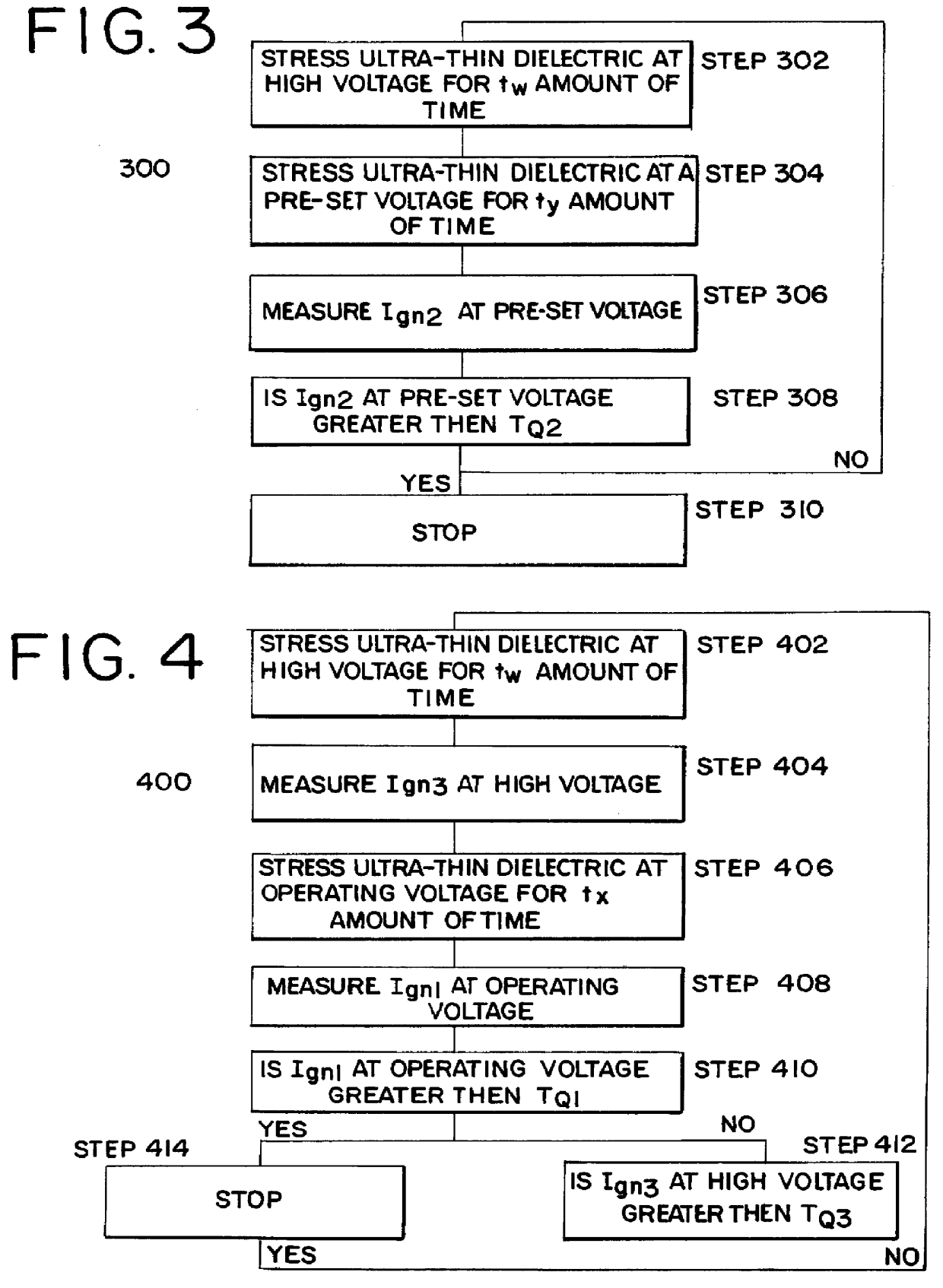
In accordance with the first embodiment, a process cycles a fluctuating electrical field bias across the ultra-thin dielectric film. The process employs a variable power source to induce a range of electrical fields from relatively low to high ele...


PUM


Abstract

An ultra-thin dielectric film is subject to a dynamic electrical bias. During a first phase, the ultra-thin dielectric film is under a high field bias generated by the application of a high voltage. The duration of the high electrical stress is dependent on the intrinsic properties of the ultra-thin dielectric material. In a second phase, the ultra-thin dielectric film is subjected to an operating field bias generated by the application of an operating voltage. The change in the field bias exposes the dielectric to a similar dynamic stress that microelectronic devices ordinarily experience. At the operating field stage, a gate current is measured and compared to a predetermined range. Once the gate current exceeds that range the test concludes. Otherwise, the test cycles between the above-mentioned phases for a predetermined number of iterations based on prior experimental correlation. In a destructive testing mode, the process is continuous and does not conclude until the gate current exceeds a predetermined range. The ultra-thin dielectric gate current may also be measured as the ultra-thin dielectric is heated so that the transport properties or reliability of the ultra-thin dielectric is more clearly understood.

Description

1. Technical Field of the InventionThe present invention relates to the reliability of ultra-thin dielectric films, such as mica, silicon dioxide, or Teflon, in semiconductor processing, and, in particular, relates to an ultra-thin dielectric process that tests the intrinsic properties of highly thin dielectric films at their operating field bias.2. Description of Related ArtUltra-thin dielectric films have been used extensively as insulating layers and protective barriers in microelectronic circuits. Conventional micro-electronic circuits are made of substrates, conductive bands, and highly thin dielectric materials. The reliability of ultra-thin dielectric affects the overall reliability of microelectronic circuits. Because an ultra-thin dielectric failure can result in catastrophic circuit failures, there exists a need to provide a reliable ultra-thin dielectric testing device and process that are capable of predicting the reliability of ultra-thin dielectrics in a cost-effective...

Claims


Application Information

Patent Timeline
IPC IPC(8): G01R31/12
CPCG01R31/129
Inventor BANG, DAVIDXIANG, QI
Owner ADVANCED MICRO DEVICES INC
Why Eureka
Try Eureka