Cleaning methods of porous surface and semiconductor surface

a technology of porous silicon substrate and cleaning method, which is applied in the direction of cleaning process and apparatus, cleaning process using liquids, chemistry apparatus and processes, etc., can solve the problems of difficult elimination of chemicals, damage to fine patterns, and inability to avoid porous silicon substrates, etc., and achieve the effect of efficient removal of dust particles adhesion

Inactive Publication Date: 2000-05-09
CANON KK
View PDF9 Cites 93 Cited by
  • Summary
  • Abstract
  • Description
  • Claims
  • Application Information

AI Technical Summary

Benefits of technology

An object of the present invention is, therefore, to provide a new cleaning method capable of efficiently removing the dust particles adhering to such a porous silicon surface without using chemicals that might affect the subsequent processes and without causing collapse of the porous silicon surface.
Since the high-frequency cleaning methods of the present invention can be easily introduced, for example, to the pure water rinse step after the conventional anodization process or after the oxidation process conducted thereafter, the introduction thereof is easy in terms of workability, cost effectiveness, and stability.

Problems solved by technology

It is well known that, cleaning is indispensable before and after processing in the semiconductor processes and that it is also unavoidable in the case of the porous silicon substrate.
Low-frequency cleaning causes damage to fine patterns due to the cavitation impact and is no longer used in the semiconductor processes of 4-Mbit DRAM and processes.
Therefore, use of chemicals in conventional chemical wet cleaning causes the chemicals to intrude deeply into the pores, which makes complete elimination of chemicals difficult even with rinsing with pure water for a long time.
It negatively affects the post-processes like the epitaxial growth on the porous structure.
The reason why the positive cleaning of porous silicon surface has not been conducted heretofore is believed to be the above problem.
Such high numbers are, however, anomalous numbers when compared with those in the current semiconductor processes, wherein the dust particles are removed down to several or less particles on the surface of a bulk substrate after RCA-cleaning.
These dust particles adhering during anodization can be decreased to some extent by liquid circulation of the above electrolyte solution and collection of dust particles with a filter, but the decrease is not sufficient yet.
Therefore, prevention of adhesion of the dust particles is not easy.
As a matter of course, such dust particles the generate imperfections in the subsequent processes, such as anomalous growth or pinholes in the film-forming process, and were problematic in applications of porous silicon.

Method used


Image

  • Cleaning methods of porous surface and semiconductor surface
  • Cleaning methods of porous surface and semiconductor surface
  • Cleaning methods of porous surface and semiconductor surface

Examples


embodiment 2

(Embodiment 2)

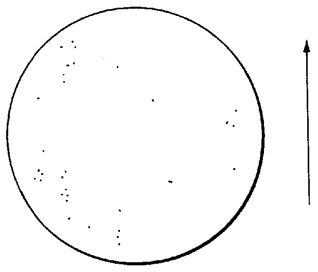
As described previously, it was found by the research of the present inventors that even several hundred dust particles not less than 0.3 .mu.m, obtained from the laser reflection intensity distribution, adhered

to the surface of a porous silicon substrate having the porous structure which was made by anodization and rinsed with pure water, in the 5-inch-diameter wafer (FIG. 28). The conceivable causes of adhesion of dust particles include dust mixed in the anodization apparatus and in the electrolyte solution and the dust generated by the workers during the process, and it is also conceivable that the porous silicon surface becomes hydrophobic because of anodization in the high-concentration hydrofluoric electrolyte solution, so that the silicon substrate becomes easy to charge electrostatically so as to adsorb dust particles. Therefore, prevention of adhesion of dust particle is not easy.

Since the porous structure is fine and dense and has long pores, use of chemicals...

embodiment 1

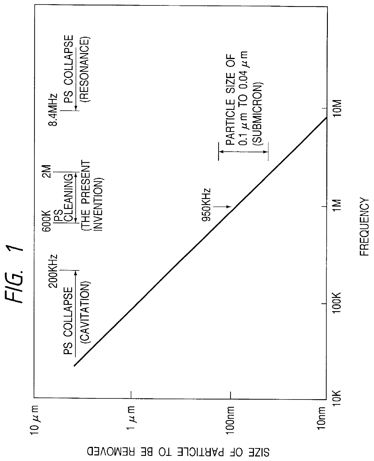
cleaning method of the fine and fragile porous structure, for which no preferred cleaning method had existed before, and was the method for cleaning the surface of a porous structure with the pure water on which the high-frequency ultrasonic wave, the frequency of which is in the range of from 200 kHz to 8.4 MHz, preferably in the range of from 600 kHz to 2.0 MHz, more preferably in the range of from 800 kHz to 1.6 MHz, is superimposed.

When ultrasonic cleaning is carried out with pure water, bubbles are generated in the pure water in the high-frequency case, especially, and those bubbles adhere to the porous silicon surface having a hydrophobic surface after removal of a surface oxide film.

The bubbles adhering to the surface are not easy to remove, especially when cleaning is made with the substrate to be cleaned being set in a pure water bath on which the ultrasonic wave is superimposed. Specifically, the small bubbles adhering to the substrate are not removed even by flowing water...

embodiment 3

(Embodiment 3)

In Embodiment 3, the porous silicon surface is subjected to a hydrophilic process and then to ultrasonic cleaning. The ultrasonic cleaning of a porous silicon surface is carried out in the high frequency band of from 200 kHz to 8.4 MHz, preferably in the range of from 600 kHz to 2 MHz. More preferably, cleaning is carried out using the high-frequency ultrasonic wave in the frequency band classified megasonic ranging from 800 kHz to 1.6 MHz, thereby avoiding the risk of collapse of the porous structure.

However, observed in the above-stated cleaning method by the present inventors is the phenomenon that bubbles are also generated from the pure water in the case of application of high-frequency ultrasonic waves and that the bubbles adhere, particularly, to the hydrophobic substrate surface.

The bubbles impede propagation of ultrasonic waves so as to degrade the cleaning effect and draw fine dust particles in the pure water to the gas-liquid interface, so as to contaminate ...


PUM

PropertyMeasurementUnit
frequencyaaaaaaaaaa
frequencyaaaaaaaaaa
frequenciesaaaaaaaaaa

Abstract

Provided is a suitable cleaning method of a porous semiconductor substrate without collapse of the porous structure due to cavitation or resonance. In a cleaning method of a porous surface of a semiconductor substrate having the porous structure at least in the surface, cleaning for removing dust particles adhering to the porous surface of the substrate takes place with pure water on which a high-frequency wave with a frequency in the range of from 600 kHz to 2 MHz is superimposed.

Description

BACKGROUND OF THE INVENTION1. Field of the InventionThe present invention relates to a cleaning method for cleaning a substrate having a porous structure in the surface thereof and, more particularly, to a cleaning method of porous surface. The present invention is suitably applicable as a cleaning method for cleaning a porous silicon semiconductor substrate used for selective etching or dielectric isolation of a semiconductor or used as a light emitting material, which demands the most strict control of cleanliness. The invention also relates to a cleaning method of a semiconductor surface.2. Related Background ArtThe method for forming the porous structure typified by porous silicon was introduced by A. Uhlir in 1956 (Bell. Syst. Tech. J., 35, pp. 333).After that, application technologies were developed including use thereof as a selective etching layer or as an isolation area after oxidized, epitaxial growth on porous silicon, etc. The present applicant disclosed in Japanese Laid...

Claims


Application Information

Patent Timeline
Patent Type & Authority Patents(United States)
IPC IPC(8): B08B3/12H01L21/306H01L21/02H01L21/3063
CPCB08B3/12H01L21/3063H01L21/02052Y10S134/902
Inventor FUJIYAMA, YASUTOMOKUMOMI, HIDEYA
Owner CANON KK
Why Eureka
Try Eureka