Structure of a capacitor in a semiconductor device having a self align contact window which has a slanted sidewall

Inactive Publication Date: 2000-06-20
UNITED MICROELECTRONICS CORP
View PDF5 Cites 60 Cited by
  • Summary
  • Abstract
  • Description
  • Claims
  • Application Information

AI Technical Summary

Problems solved by technology

This method can increase the capacitance effectively but is difficult to be controlled to obtain a uniform and stable dielectric thin film.
For the present, to increase the size of the interfacial area, such as a fin type or a hemispheric grain type is applied but has a difficulty for massive production due to the complexity of fabrication.
On the contrary, if the temperatures used in the process of annealing is too low, and then the defect existing in the dielectric thin film could not effectively be removed.
Unfortunately, the conventional MIM capacitor usually has a thick lower electrode, on which the etching is complicate and taking time.
Except this, it has another problem that because the profile of the pitted contact window is usually steeper, it causes not only the difficulty of the alignment of a source/drain region but also the bad quality of the ability of the step coverage.
This causes the complexity of the fabrication.
1. If the thickness of the lower electrode is too thick for being able to hold more charges, the etching can no

Method used


Image

  • Structure of a capacitor in a semiconductor device having a self align contact window which has a slanted sidewall
  • Structure of a capacitor in a semiconductor device having a self align contact window which has a slanted sidewall
  • Structure of a capacitor in a semiconductor device having a self align contact window which has a slanted sidewall

Examples


Embodiment Construction

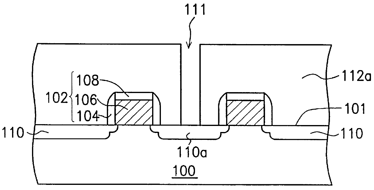
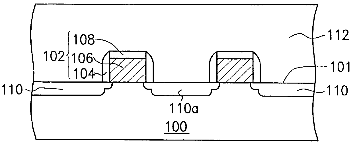
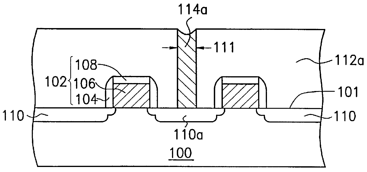
FIG. 2A through FIG. 1F illustrate the sectional plots of a capacitor of a DRAM in the fabricating procedure according to the preferred embodiments of the invention. The like marks represent the like elements in the FIGs.

Referring to 2A, two gates 202 with an identical structure but only one being marked are shown in the figure over a substrate 200 on a substrate surface 201. The FIG. 2A further includes a source / drain region 210 and a commonly used source / drain region 210a between the gates 202 under the substrate surface 201. One of gates 202 with marks has a doped polysilicon layer 206 covered by a spacer 204 and a cap layer 208. The source / drain region 210 and commonly used source / drain region 210a are the doped area with a structure of lightly doped drain (LDD) and can be formed by doing the ion implantation, in which the structure of the gates 202 is treated as the mask. A number of lightly doped areas, located on the fringe of the source / drain region 210 and the commonly used...


PUM


Abstract

A structure of a capacitor includes two gates and a commonly used source/drain region on a substrate. Then, a pitted self align contact window (PSACW) partly exposes the commonly used source/drain region. Then an glue/barrier layer and a lower electrode of the capacitor are over the PSACW. Then a dielectric thin film with a material having high dielectric constant is over the lower electrode. Then, an upper electrode is over the dielectric thin film to complete a capacitor, which has a structure of metal insulator metal with a shape like the PSACW.

Description

1. Field of the InventionThis invention relates to a structure of a capacitor in a semiconductor device, and more particularly to a structure of a capacitor in a dynamic random access memory (DRAM) device.2. Description of Related ArtFor memory devices with high integration such as DRAM devices with memory capacity of 256 Megabit, their capacitor need a dielectric thin film to be constructed as the three dimensional structures like stacked type or trench type. Thus these memory devices should have a large area of the dielectric thin film to store the charge to avoid the soft error. Utilizing a method of the low pressure chemical vapor deposition (LPCVD), which is one of applications of the chemical vapor deposition (CVD), to make the dielectric thin film made of Ta.sub.2 O.sub.5 is popular for the present because this material produces a dielectric constant about 25, which is far larger than that of oxide, and has a better ability of step coverage. The step coverage means that the c...

Claims


Application Information

Patent Timeline
IPC IPC(8): H01L21/02H01L21/70H01L21/8242H01L27/108
CPCH01L27/10852H01L28/82H10B12/033
Inventor HUANG, KUO-TAIHSIEH, WEN-YIYEW, TRI-RUNG
Owner UNITED MICROELECTRONICS CORP
Why Eureka
Try Eureka