Compositions and structures for chemical mechanical polishing of FeRAM capacitors and method of fabricating FeRAM capacitors using same

a technology of feram capacitors and compositions, applied in the field of compositions and structures for chemical mechanical polishing of feram capacitors, can solve the problems of deformation of pads, deformation of unwanted structures at the edges of electrodes, and difficult sub-micron patterning of both noble metals and ferroelectric films, so as to reduce the susceptibility of device structures to short-circuiting or high leakage current behavior

Inactive Publication Date: 2002-02-12
GULA CONSULTING LLC
View PDF6 Cites 187 Cited by
  • Summary
  • Abstract
  • Description
  • Claims
  • Application Information

AI Technical Summary

Benefits of technology

(II) metal (electrode material) or dielectric (ferroelectric or high dielectric constant) material is removed either during or after the CMP planarization to create a local recess in the substrate, optionally followed by deposition of an insulating layer thereover, to thereby reduce the susceptibility of the device structure to short-circuiting or high leakage current behavior in use, with such metal removal comprising at least one of the steps of:

Problems solved by technology

It is well known that these materials require electrodes made from noble metals or noble metal alloys such as Pt, Ir, IrO.sub.2, Pt--Ru, etc., and sub-micron patterning of both the noble metals and the ferroelectric films is very difficult because of the absence of volatile products for the elemental constituents.
State-of-the-art dry etching processes for Pt and Ir are known to have fundamental difficulties due to the predominantly physical (not chemical) mechanism for material removal, resulting in formation of unwanted structures (sometimes called "ears") at the edges of the electrodes.
Research showed that deformation of the pad resulted from the brittle, hard surfaces of the ICs structure.
Although this approach allowed the same pads to be used for an extended period of time, it also resulted in other complications.
Most conventional pads consist of "pockets" within the polyurethane which are prone to clogging due to the residual debris discharged during the process.
The foregoing factors add complexity to IC design.
If IC manufacturing processes will utilize CMP processing, device dimensions and density are critical and require close scrutiny.
The purpose of the slurry is simple, yet understanding and modeling all the mechanical and chemical reactions involved is extremely difficult.
The top oxidized metal layer is more brittle and easily removed with the embedded abrasive particles.
If the oxidation potential is too aggressive or the resulting metal compound too soluble, metal corrosion can occur as a result of wet etching.
Two other key issues relating to the choice of slurry deal with post-CMP clean-up and the introduction of mobile ions to the wafer.
Although CMP has revolutionized global planarization technology, some significant problems exist.
One of the major difficulties is in-situ measuring of the amount of material removed from the wafer surface.
Due to inaccurate models, many results of CMP machines are difficult to reproduce and the machines themselves do not exhibit the ability for precise process control.
This also leads to difficulty in analyzing feedback, or using in-situ measurements, to make adequate and appropriate process alterations to alleviate process complications.
Such efforts will aid in more precisely controlling the entire CMP process, but the analysis techniques and instruments have not been developed to a state of high commercial precision.
Further, the CMP pad does not remove material uniformly as the pad wears.
These factors make it difficult to maintain an acceptable removal rate and uniformity in the CMP operation.
A large degree of mechanical removal of the noble metals and oxide films is necessary to achieve high removal rates, and the CMP process may result in physical or chemical damage to the capacitor layers.
Physical damage includes disruption of the microstructure and long range order of the polycrystalline oxide lattice, which is principally responsible for the unique properties of the ferroelectric and high .epsilon. oxides.
Chemical damage, especially in the ferroelectric layer, may involve removal of specific cations, interdiffusion, de-oxygenation, or introduction of metallic contamination from the polishing media.
One difficulty in the use of CMP for planarization of FeRAM and high permittivity capacitor structures is the difficulty of accurately controlling the removal of oxide materials such as silicon dioxide (SiO.sub.2).
Damage to the ferroelectric or metal layers will therefore have large effects on the functionality of the capacitor.

Method used


Image

  • Compositions and structures for chemical mechanical polishing of FeRAM capacitors and method of fabricating FeRAM capacitors using same
  • Compositions and structures for chemical mechanical polishing of FeRAM capacitors and method of fabricating FeRAM capacitors using same
  • Compositions and structures for chemical mechanical polishing of FeRAM capacitors and method of fabricating FeRAM capacitors using same

Examples


Embodiment Construction

The disclosure of U.S. patent application No. 08 / 975,366 filed Nov. 20, 1997 in the names of Peter C. Van Buskirk and Peter S. Kirlin for "Chemical Mechanical Polishing of FeRAM Capacitors" and issued as U.S. Pat. No. 5,976,928 on Nov. 2, 1999, hereby is incorporated herein by reference in its entirety.

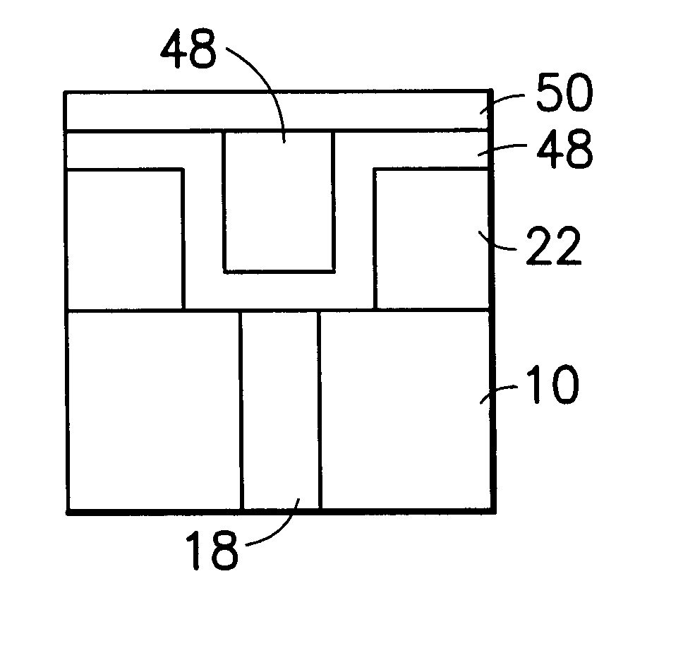
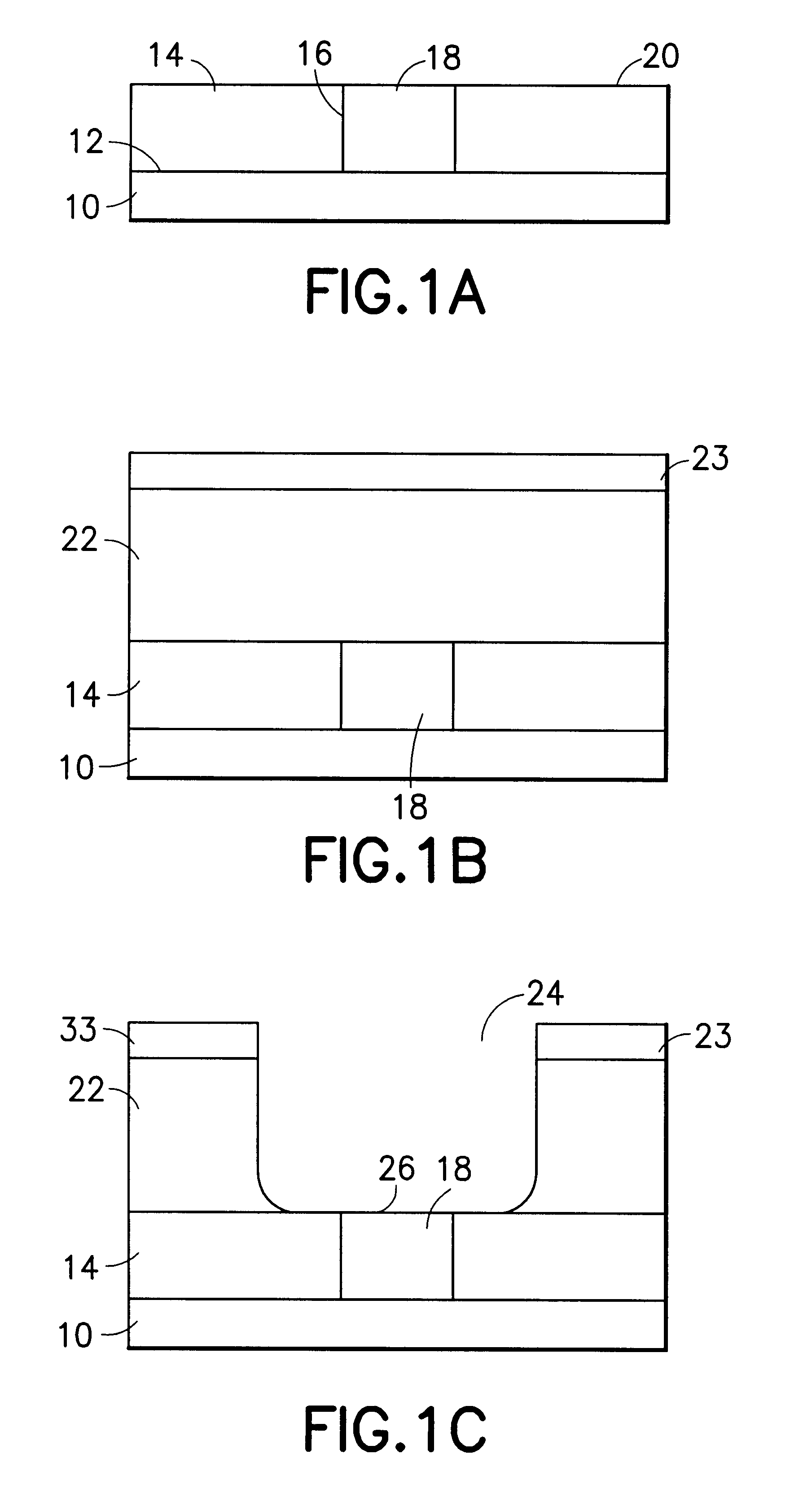
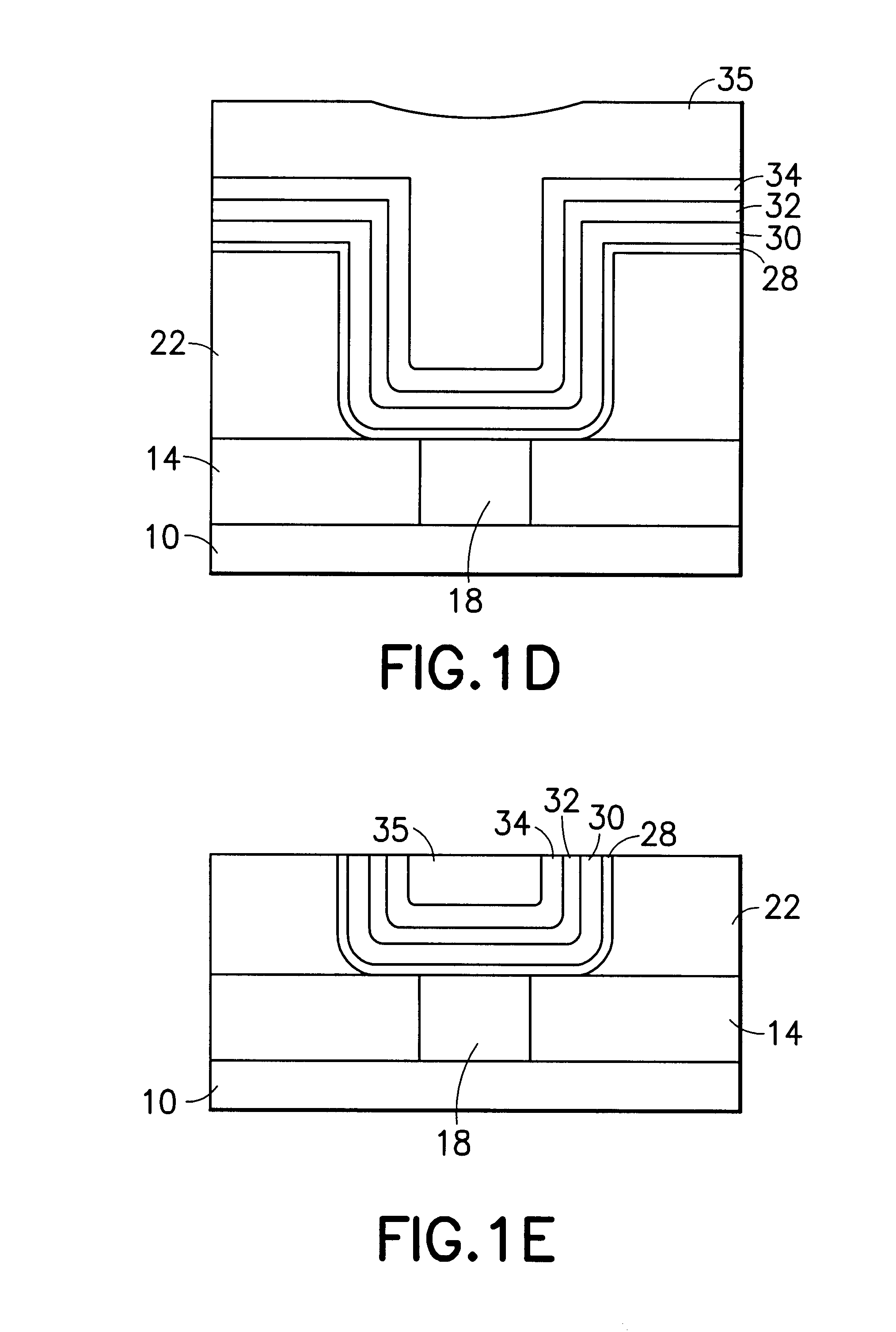
The method of the present invention permits the formation of a microelectronic device structure including forming a capacitor recess dielectric material and device structure materials on a substrate, in which the device structure materials are removed during processing to a planarization depth therein by chemical mechanical polishing (CMP). In accordance with the invention, the capacitor recess dielectric material is formed to contain a stop layer at the desired planarization depth in the dielectric insulating material. The stop layer has a substantially lower CMP removal rate than the dielectric insulating material under CM, conditions, so that the removal of the device structure mat...


PUM

PropertyMeasurementUnit
sizeaaaaaaaaaa
sizeaaaaaaaaaa
sizeaaaaaaaaaa

Abstract

An integrated circuit structures formed by chemical mechanical polishing (CMP) process, which comprises a conductive pathway recessed in a dielectric substrate, wherein the conductive pathway comprises conductive transmission lines encapsulated in a transmission-enhancement material, and wherein the conductive pathway is filled sequentially by a first layer of the transmission-enhancement material followed by the conductive transmission line; a second layer of transmission-enhancement material encapsulating the conductive transmission line and contacting the first layer of the transmission-enhancement material, wherein the transmission-enhancement material is selected from the group consisting of high magnetic permeability material and high permittivity material. Such integrated circuit structure may comprise a device structure selected from the group consisting of capacitors, inductors, and resistors. Preferably, the transmission-enhancement material comprises MgMn ferrites, MgMnAl ferrites, barium strontium titanate, lead zirconium titanate, titanium oxide, tantalum oxide, etc.

Description

1. Field of the InventionThe present invention relates to a chemical mechanical polishing (CMP) method and composition having applicability to the manufacture of ferroelectric random access memory capacitors, in which a stop layer is employed over the capacitor recess dielectric material to achieve the required planarization of the microelectronic device structure. It is also applicable to the fabrication of other integrated circuit structures, such as capacitor, resistor and inductor structures, which in utilizing multilayer geometries benefit from the inherently planarizing character of CMP.2. Description of the Related ArtThere is currently a major effort in semiconductor companies, worldwide, to commercialize high dielectric constant and ferroelectric thin films in advanced DRAMs and ferroelectric random access memories (FeRAMs), respectively. These material s include BaSrTiO.sub.3 (BST) for DRAMs and PbZrTiO.sub.3 (PZT) and SrBi.sub.2 Ta.sub.2 O.sub.9 (SBT) for FeRAMs.It is wel...

Claims


Application Information

Patent Timeline
Patent Type & Authority Patents(United States)
IPC IPC(8): H01L21/02H01L21/70H01L21/8242H01L21/302C09G1/02C09K3/14H01L21/304H01L21/3065H01L21/3105H01L21/321H01L21/768H01L21/8246H01L27/105
CPCC09G1/02C09K3/1463H01L21/31053H01L21/3212H01L28/55H01L27/1085H01L28/75H01L27/10852H01L27/10861H01L28/60H10B12/03H10B12/038H10B12/033B82Y10/00H10B99/00
Inventor VAN BUSKIRK, PETER C.RUSSELL, MICHAEL W.BILODEAU, STEVEN M.BAUM, THOMAS H.
Owner GULA CONSULTING LLC
Why Eureka
Try Eureka