

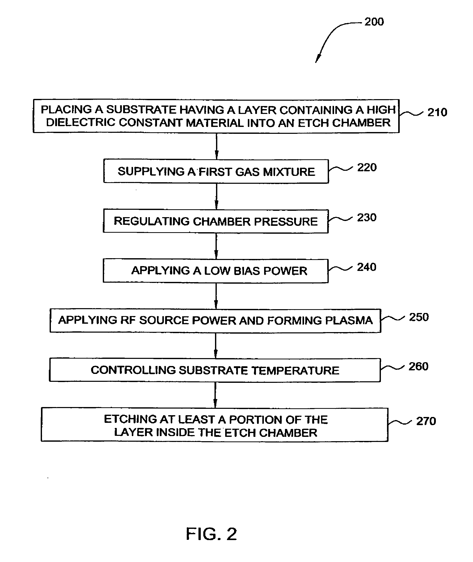
Etching high-kappa dielectric materials with good high-kappa foot control and silicon recess control
a dielectric material and high-kappa technology, applied in the field of dry etching of semiconductor substrates, can solve the problems of void space, difficulty in etching even a thin layer of high- material using conventional silicon oxide etchants, and improper operation of the resistor or its defective state, so as to reduce gas chemistries and high selectivity
- Summary
- Abstract
- Description
- Claims
- Application Information
AI Technical Summary
Benefits of technology
Problems solved by technology
Method used
Image

Examples
example 1
[0055] A substrate is loaded onto the substrate support of an etch chamber and a hafnium oxide layer was etched using a gas mixture of about 40 sccm chlorine gas and about 40 sccm carbon monoxide, and argon, having a chamber pressure of about 4 mTorr and a substrate temperature of about 250 degrees Celsius. No pedestal bias power was applied to the substrate support and a RF power of about 1100 Wafts at a frequency of 13.56 MHz was applied to an antenna source to form a plasma. The hafnium-oxide layer was etched by the Cl2 / CO chemistry at an etch rate of about 100 Å / min having an etch selectivity to SiO2 of greater than 30:1. The etch selectivity to polysilicon is greater than 3:1.
[0056] The result of the etching process is shown in FIG. 6A, illustrating a silicon dioxide substrate 604, an etched high-κ dielectric material layer 606, and a polysilicon layer 608. As shown in FIG. 6A, the etched high-κ dielectric material layer 606 includes a high-κ foot 620 which is undesirable for ...
example 2
[0058] A substrate is loaded onto the substrate support of an etch chamber and a hafnium oxide layer was etched using a gas mixture of about 40 sccm chlorine gas and about 40 sccm carbon monoxide, and argon, having a chamber pressure of about 4 mTorr and a substrate temperature of about 250° C. No bias power was applied to the substrate support and a high RF source power of about 1000 Watts was applied to an antenna source to form a plasma.
[0059] The result of the etching process is shown in FIG. 7A, illustrating a silicon dioxide substrate 704, an etched high-κ dielectric material layer 706, and a polysilicon layer 708. The etched high-κ dielectric material layer 706 includes a void space 730 (silicon recess) showing the attack of the silicon dioxide substrate 704 by the etch process which is undesirable for most semiconductor applications.
[0060] As a comparison, a low source power of about 400 Watts was used in addition to the Cl2 / CO chemistry under the same process parameters a...
example 3
[0061] A substrate is loaded onto the substrate support of an etch chamber and a hafnium oxide layer was etched using a two-step etch process. The etch process include a first gas mixture of about 100 sccm chlorine gas and about 5 sccm methane, and argon, having a chamber pressure of about 10 mTorr and a substrate temperature of about 250° C. No bias power was applied using the first gas mixture and a plasma was formed to etch a portion of the hafnium oxide layer. The hafnium-oxide layer was etched by the Cl2 / CH4 chemistry at a rate of about 100 Å / min having an etch selectivity to SiO2 of greater than 10:1. The etch selectivity to polysilicon is greater than 3:1.
[0062] Next, a second gas mixture having about 40 sccm chlorine gas and about 40 sccm carbon monoxide, and argon, is used in the presence of a RF source power of about 400 Watts to form a plasma. The hafnium-oxide was etched by the Cl2 / CO chemistry at a rate of about 50 Å / min having an etch selectivity to SiO2 of greater th...
PUM
| Property | Measurement | Unit |
|---|---|---|
| Temperature | aaaaa | aaaaa |
| Temperature | aaaaa | aaaaa |
| Power | aaaaa | aaaaa |
Abstract
Description
Claims
Application Information