Method for making y-shaped multi-fin stacked capacitors for dynamic random access memory cells

a technology of dynamic random access memory and stacked capacitors, which is applied in the direction of capacitors, semiconductor devices, electrical equipment, etc., can solve the problems of reducing the performance (speed) of dram circuits, increasing the difficulty of fabricating stacked or trench storage capacitors with sufficient capacitance,

Inactive Publication Date: 2000-07-04
TAIWAN SEMICON MFG CO LTD
View PDF12 Cites 15 Cited by
  • Summary
  • Abstract
  • Description
  • Claims
  • Application Information

AI Technical Summary

Problems solved by technology

Unfortunately, as the cell size decreases, it becomes increasing more difficult to fabricate stacked or trench storage capacitors with sufficient capacitance to store the necessary charge t

Method used


Image

  • Method for making y-shaped multi-fin stacked capacitors for dynamic random access memory cells
  • Method for making y-shaped multi-fin stacked capacitors for dynamic random access memory cells
  • Method for making y-shaped multi-fin stacked capacitors for dynamic random access memory cells

Examples


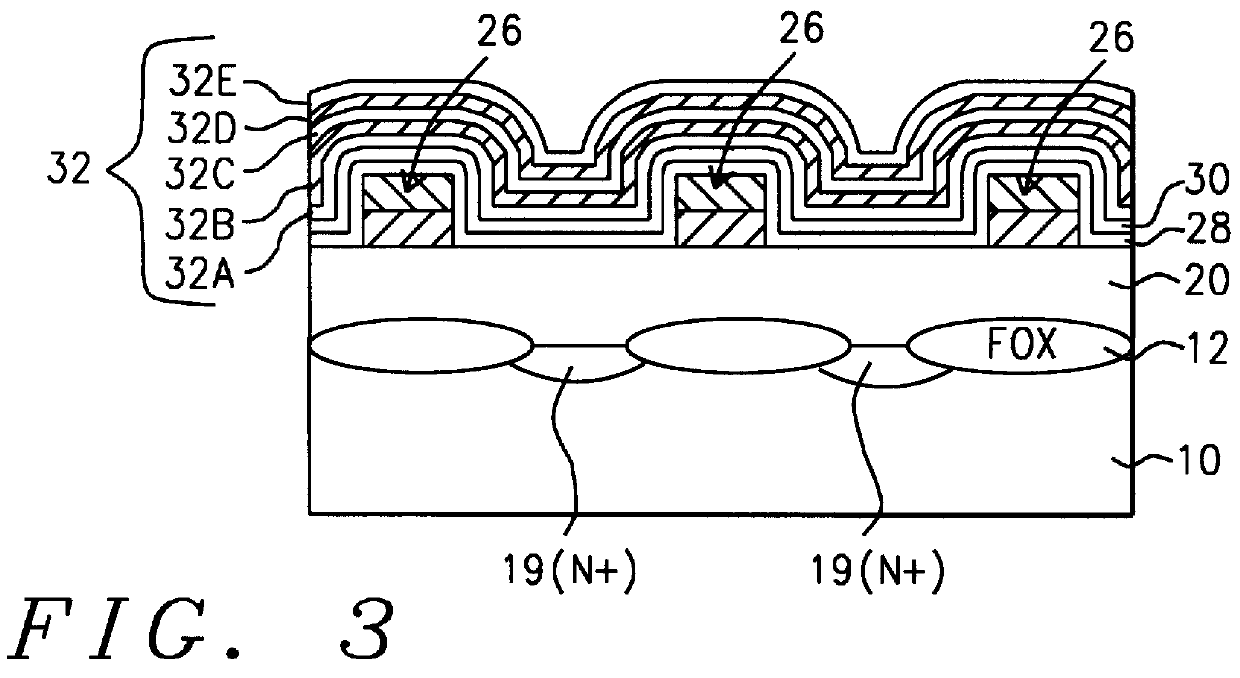
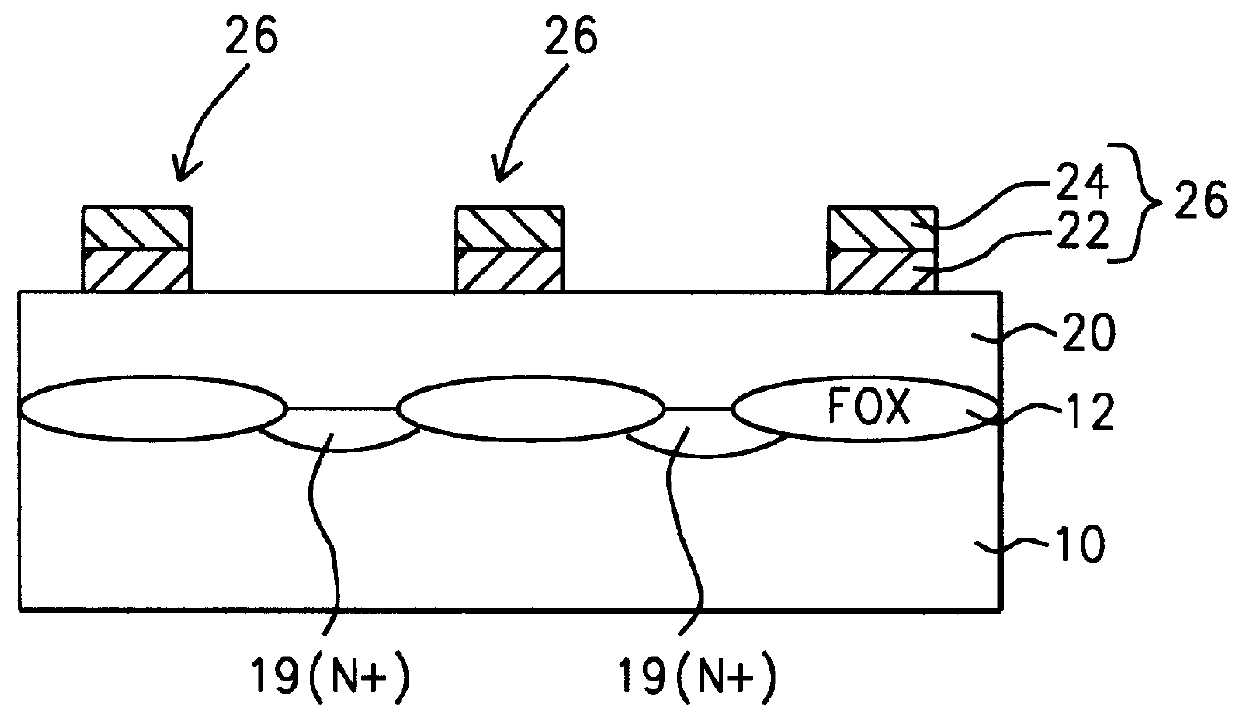
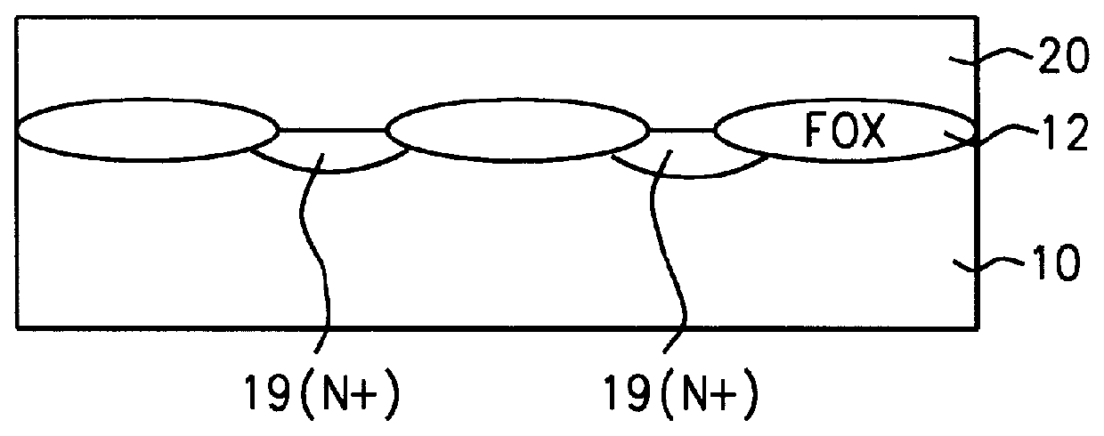
Embodiment Construction

To better appreciate this invention, DRAM cells were fabricated on silicon wafers using the above processing steps to make the Y-shaped three-fin stacked capacitors having increased capacitance, and control wafers were processed to make the T-shaped three-fin stacked capacitors. The capacitance was measured on the Y-shaped capacitors and on the T-shaped capacitors using a capacitance meter, Model 490-8AU, manufactured by MDC Company of U.S.A.

The following Table shows the comparison of the capacitance measured on the Y-shaped three-fin capacitors of this invention with the T-shaped three-fin capacitors. The measurements were made on 52 test sites across the wafers, and the mean value of the capacitance is shown in the Table below for both the Y-shaped and T-shaped capacitors.

Row 1 shows the wafer identification number, row 2 shows the thickness of the interelectrode dielectric layer, and row 3 shows the measured capacitance in femtoFarads (fF). As can be seen from the Table, the capa...


PUM


Abstract

An array of DRAM cells having Y-shaped multi-fin stacked capacitors with increased capacitance is achieved. A planar first insulating layer is formed over the semi-conductor devices on the substrate. Polycide bit lines are formed on the first insulating layer, and a second insulating layer and a silicon nitride (Si3N4) etch-stop layer are conformally deposited. A multilayer, composed of a alternating insulating and polysilicon layers, is conformally deposited over the bit lines. Capacitor node contact openings are etched in the multilayer and in the underlying layers to the substrate. A fourth polysilicon layer is deposited sufficiently thick to fill the node contact openings and to form the node contacts. The multilayer is then patterned to leave portions over the node contacts, and an isotropic etch is used to remove the insulating layers exposed in the sidewalls of the patterned multilayer to provide Y-shaped multi-fin capacitor bottom electrodes over the bit lines. These Y-shaped multi-fin capacitors increase the capacitance by 37% over T-shaped multi-fin capacitors. The DRAM capacitors are then completed by forming an interelectrode dielectric layer on the bottom electrodes and by depositing a fifth polysilicon layer to form the capacitor top electrodes.

Description

(1) FIELD OF THE INVENTIONThe present invention relates to semiconductor integrated circuits, and more particularly to a method for fabricating an array of dynamic random access memory (DRAM) cells with Y-shaped stacked capacitors to increase the capacitance while maintaining a high density of memory cells.(2) DESCRIPTION OF THE PRIOR ARTDynamic random access memory (DRAM) circuits (devices) are used extensively in the electronics industry, and more particularly in the computer industry for storing data in binary form (1 and 0) as charge on a storage capacitor. These DRAM devices are made on semiconductor substrates (or wafers) and then the substrates are diced to form the individual DRAM circuits (or chips). Each DRAM circuit (chip) consists in part of an array of individual memory cells that store binary data (bits) as electrical charge on the storage capacitors. Further, the information is stored and retrieved from the storage capacitors by means of switching on or off a single a...

Claims


Application Information

Patent Timeline
IPC IPC(8): H01L21/8242H01L21/70H01L21/02
CPCH01L27/10855H01L28/87H01L27/10885H10B12/0335H10B12/482
Inventor LIN, YO-SHENGLIU, HSIEN-TSUNG
Owner TAIWAN SEMICON MFG CO LTD
Why Eureka
Try Eureka