Method for fabricating a very dense chip package

a chip package and very dense technology, applied in the direction of electrical equipment, semiconductor/solid-state device details, semiconductor devices, etc., can solve the problems of increasing the maximum chip size, occupying valuable space on the semiconductor substrate, and the physical limits of present-day fabrication equipment, etc., to achieve constant width, reduce height, and increase width

Inactive Publication Date: 2000-07-11
GOOGLE LLC
View PDF30 Cites 60 Cited by
  • Summary
  • Abstract
  • Description
  • Claims
  • Application Information

AI Technical Summary

Benefits of technology

Further, at least one metallic interconnect (eg, metalization layer) is disposed at or over the two top faces, so as mechanically and electrically to provide an interconnect between circuit devices residing on the neighboring chips. Parts of the metallic interconnect, at least at or over the selected portions of the top faces, have a substantially constant width--e.g., without limitation, approximately 5 .mu.m. Preferably, the interconnect at a location over the gap has a greater width (e.g., +20% to +100%), to compensate for any thinning (reduced height) of the interconnect that may have occurred during a metallization process to provide the interconnect. For example, over the gap, the interconnect preferably has a rounded or a button-like shape having a maximum diameter of approximately 6 .mu.m when the other parts of the interconnect have a maximum width of approximately 5 .mu.m.
The present inventors believe that, for neighboring chips having top surfaces which are not co-planar, the metallic interconnect provided over a gap of greater than about one .mu.m is less likely to break, and is more likely to possess a greater bandwidth (eg, higher data rates), than when the features of this additional embodiment are not present in the chip arrangement.
As endowed with the very dense chip-to-chip placement that can be provided by the present invention, a reduction in signal delays between chips is achieved. Also, the subsequent metallization interconnect can be done with standard hard mask back-end-of-line (BEOL) technology in standard process lines, thereby at least reducing the number of C4's needed as interconnect means through supporting package substrates.
The inventive packaging scheme also reduces the number of I / O's, reconstitutes chip yields, reduces chip power requirements, allows chip mixing, allows erector-set type chip building opportunities and can effectively accommodate chips having different heights (thicknesses).
For instance, the invention provides for smaller chips to be placed on a carrier substrate to permit higher yields. Also, different chips can be optimized in standard (e.g., DRAM, SRAM, Logic, and so forth) process lines before their marriage with other chips from other process lines, on a common carrier substrate, as opposed to attempting to use one large chip containing all elements of the final chip. Using such smaller chips as "chip sectors" in this way, the chip sectors can be separately pre-tested for quality and functionality before final placement on a common substrate, thereby optimizing final chip yields. The present invention also allows for a mix and match approach to chip placement with each other on a carrier substrate to realize large chip hybrids (e.g., GaAs with SOI, DRAM with Logic, and so forth). Thus, for example, chips having different primary electronic functions (e.g., microprocessors, main memories, non-volatile memories etc.) can be located on a common carrier substrate to realize various chip hybrid arrangements.
Also, the present invention allows elimination of electrostatic disharge system (EDS) circuits, thereby reducing power requirements. The inventive chip-and-substrate package is considered especially well-suited, e.g., for use in mobile communication and large area microprocessor chips.

Problems solved by technology

However, there are practical problems associated with continually increasing the maximum chip size.
A first set of problems relates to the physical limits of present day fabrication equipment.
While a mask larger than the lithography exposure field of the equipment can be split into multiple smaller masks that are "stitched" together to effectively multiply the size of the lithography exposure field, such "stitching" introduces undesired inaccuracies and occupies valuable space on the semiconductor substrate.
However, such a solution would require massive financial investment in research and development.
Another problem relates to a general trend of wafer yields decreasing with increasing chip size. FIG. 1 summarizes different manufacturing chip yields as a function of a chip edge dimension (square chips).
The decrease in yield with increasing chip size can be attributed to the fact that, for the same quality of semiconductor, any defect existing in a larger chip results in an overall greater area waste than is the case with smaller chip wafers.
As chip size increases, the cost of manufacturing because of yield degradation becomes prohibitive.
However, such MCMs tend to be extremely expensive because of their multilayered ceramic features and of their significantly more area requirement than the net overall area requirement of the combined set of chips.
However, the HDI technology offers poor positional accuracy of chips, preventing the use of a fixed mask to make chip-to-chip connections, and thereby making the process of interconnecting individual chips extremely time consuming and expensive.

Method used


Image

  • Method for fabricating a very dense chip package
  • Method for fabricating a very dense chip package
  • Method for fabricating a very dense chip package

Examples


Embodiment Construction

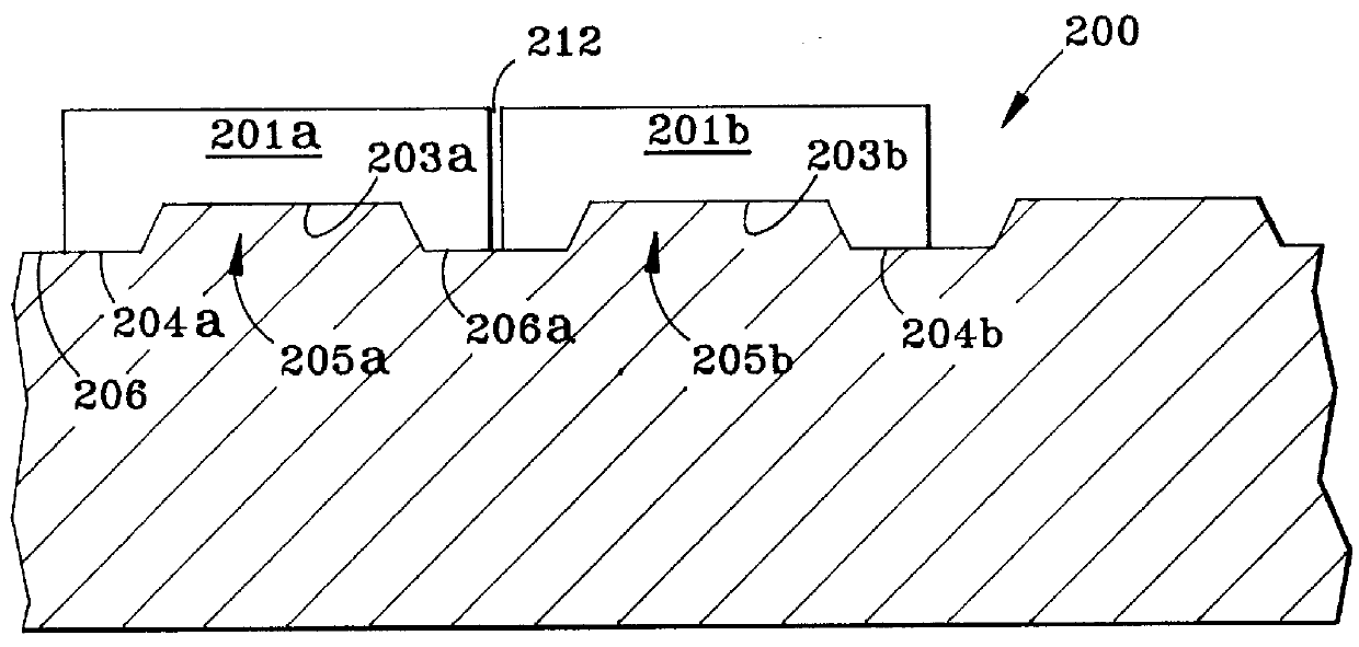
With reference to FIG. 2A, a chip-on-substrate assembly 200 of the invention is shown in which integrated circuit chips 201a,b are positioned on a carrier substrate 202 by interfitting surface depressions 203a,b on bottom faces 204a,b of the chips 201a,b with corresponding projections 205a,b extending from an upper face 206 of the carrier substrate 202. Although two chips are shown as positioned on the substrate for illustrative purposes, it will be understood that the present invention encompasses positioning a single chip or a plurality of chips on a substrate. Each of the chip depressions 203a,b can be a two-walled trench or a four-sided well configuration, where the carrier substrate projections 205a,b will have a corresponding configuration of either an upraised ridge or a mesa-like structure, respectively.

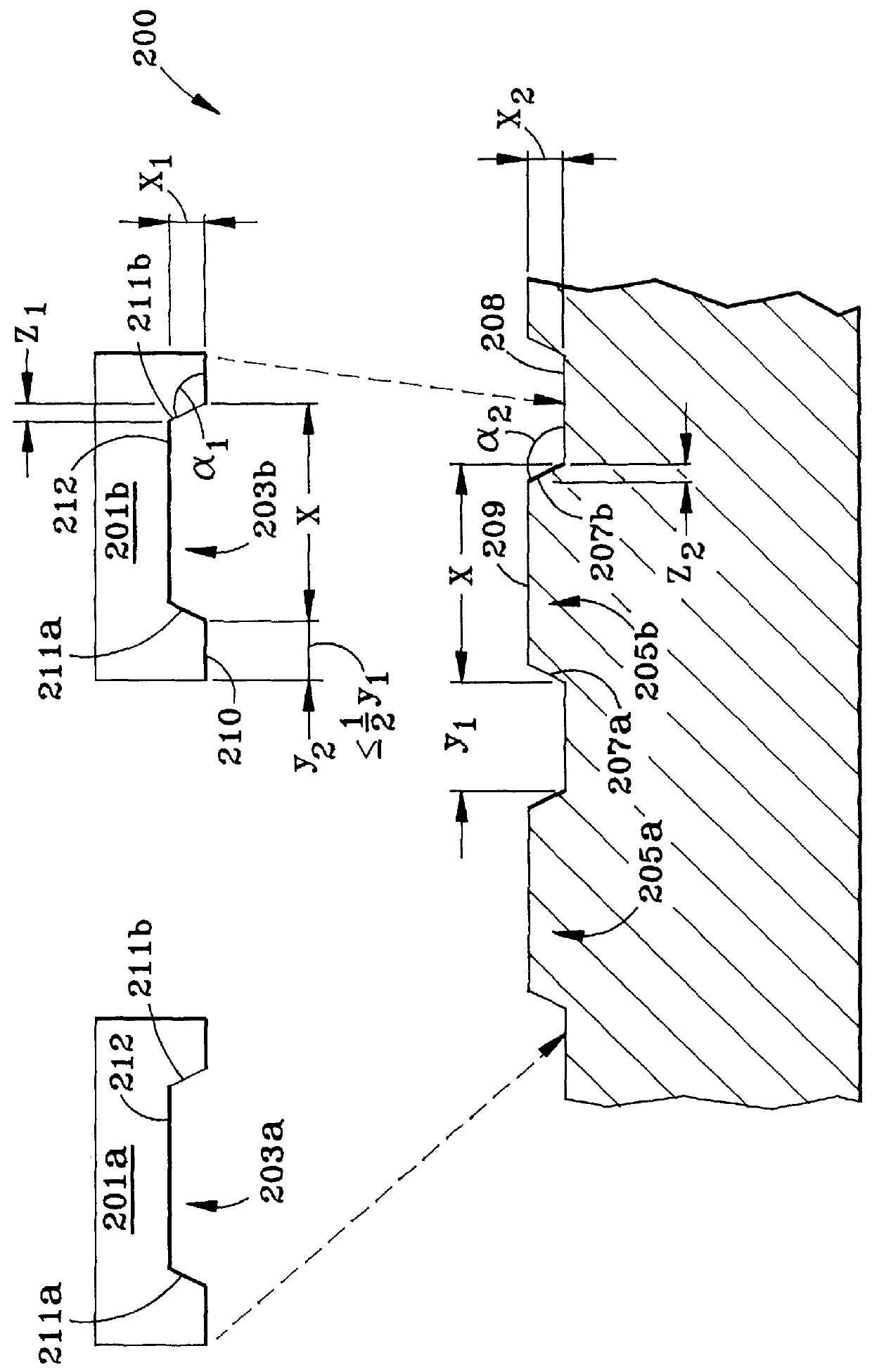
As shown in FIG. 2B, and by reference to chip 201b and projection 205b for sake of simplicity, the projection 205b has a lateral dimension "x" extending from where a first sl...


PUM


Abstract

A method for fabricating an integrated circuit package or arrangement includes providing a carrier having a surface topography of projections or recesses for supporting individual semiconductor circuit chips having conversely matching bottom surface topographies to permit self-aligned positioning of the chip on the carrier. Chips are provided such that top faces of neighboring chips lie substantially in planes separated by a distance of greater than 0.0 mu m. The carrier is arranged and dimensioned such that the neighboring chips are separated by a gap G or spacing in a range of 1 mu m<G</=100 mu m. A metallic interconnect is provided over the top faces and the gap. Preferably, the interconnect has a gradual slope over the gap.

Description

1. Field of the InventionThis invention relates to an integrated circuit arrangement such as a chip packaging configuration.2. Description of the Related ArtAs advances in semiconductor processing occur, the scale of individual integrated circuit devices continues to shrink, making it possible to incorporate increasing amounts of functionality in a single integrated circuit chip. For example, sixteen 1 MBIT Dynamic Random Access Memory (DRAM) chips of equal size in 1984 required a total chip area of 800 mm.sup.2, while a single 16 MBIT design containing the same functionality in 1990 required only 110 mm.sup.2. Thus, although the individual chip size has increased by approximately 50%, the net chip density on such chips has increased by a significant factor. Accordingly, as integrated circuit chips are required to incorporate more and more functionality, the sizes of the chips have been steadily increasing.However, there are practical problems associated with continually increasing ...

Claims


Application Information

Patent Timeline
Patent Type & Authority Patents(United States)
IPC IPC(8): H01L21/768H01L23/12H01L21/98H01L21/70H01L23/13H01L25/065H01L29/06
CPCH01L21/76838H01L23/13H01L24/18H01L24/82H01L25/0655H01L25/50H01L29/0657H01L2224/13022H01L2224/18H01L2924/01015H01L2924/01027H01L2924/01032H01L2924/01039H01L2924/01074H01L2924/10158H01L2924/10329H01L2924/14H01L2924/15153H01L2924/15157H01L2924/15165H01L2924/3025H01L2924/01005H01L2924/01006H01L2924/01019H01L2924/01023H01L2924/01033H01L2924/01055H01L2924/014H01L2224/83141H01L24/24H01L24/97H01L2224/24137H01L2224/73267H01L2224/97H01L2924/00014H01L2924/12042H01L2924/15156H01L2224/83H01L2924/00H01L2224/0401
Inventor POGGE, H. BERNHARDDAVARI, BIJANGRESCHNER, JOHANNKALTER, HOWARD L.
Owner GOOGLE LLC
Why Eureka
Try Eureka