Procedures and apparatus for turning-on and turning-off elements within a field emission display device

a technology of field emission display device and process, which is applied in the direction of tubes with screens, tubes/lamp factory adjustment, instruments, etc., can solve the problems of high probability of small ionic pressure zone, small amount of contaminants in fed vacuum tubes, and high probability of contamination forming small ionic pressure zones, etc., to achieve the effect of slowing down the emission curren

Inactive Publication Date: 2000-08-15
CANON KK
View PDF7 Cites 16 Cited by
  • Summary
  • Abstract
  • Description
  • Claims
  • Application Information

AI Technical Summary

Benefits of technology

The present invention provides for a method of removing contaminant material in newly fabricated field emission displays. According to one embodiment of the present invention, contaminant particles are removed by a conditioning process, which includes the steps of: a) driving an anode of a field emission display (FED) to a predetermined voltage; b) slowly increasing an emission current of the FED after the anode has reached the predetermined voltage; and c) providing an ion-trapping device for catching the ions and contaminants knocked off by emitted electrons. In this embodiment, by driving the anode to the predetermined voltage and by slowly increasing the emission current of the FED, contaminant particles are effectively removed without damaging the FED.
The present invention also provides for a method of operating FEDs to prevent gate-to-emitter current during turn-on and turn-off. In this embodiment, the method includes the steps of: a) enabling the anode display screen; and, b) enabling the electron-emitters a predetermined time after the anode display screen is enabled. In this embodiment, by allowing sufficient time for the anode display screen to reach a predetermined voltage before the emitter is enabled, the emitted electrons will be attracted to the anode. In this way, gate-to-emitter current is effectively eliminated when an FED is turned on. In the present embodiment, the anode display screen is enabled by applying a predetermined high voltage to the display screen, and the electron-emitters are enabled by driving appropriate voltages to the gate electrodes and emitter electrodes of the FED.
In yet another embodiment of the present invention, the method of operating field emission displays to prevent gate-to-emitter current includes the steps of: a) disabling the emitters for a predetermined time; and, b) disabling the anode display screen after the electron-emitters are disabled. In this embodiment, by allowing sufficient time for the electron-emitters to be disabled before disabling the anode display screen, all remaining electrons will be attracted to the anode. In this way, gate-to-emitter current is eliminated during a turn-off sequence of the FED. In the present embodiment, the anode display screen is disabled by applying a ground voltage to the anode of the FED, and the electron-emitters are disabled by driving the gate electrodes and the emitter electrodes to the ground voltage.
Embodiments of the present invention include the above and further include a method of operating a field emission display, the method comprising the steps of: providing the field emission display with electron-emissive elements for emitting electrons, a gate electrode for controlling electron emission from the electron-emissive elements, and a display screen for collecting the electrons; enabling the display screen to establish a voltage differential between the display screen and the electron-emissive elements; and following enabling of the display screen, enabling the gate electrode by delaying substantial electron emission from the electron-emissive elements until the voltage differential has been established to direct the electrons towards the display screen and to substantially prevent the electrons from striking the gate electrode.
Embodiments of the present invention further include a field emission display device comprising: a baseplate; a plurality of electron-emissive elements on the baseplate; a gate electrode on the baseplate for controlling electron emission from the electron-emissive elements; a display screen spaced from the baseplate and configured for collecting electrons emitted from the electron-emissive elements to generate an image thereon; and a control circuit configured to control a flow of electrons to the electron-emissive elements, the control circuit allowing a voltage differential to be established between the display screen and the electron-emissive elements prior to substantial electron emission from the electron-emissive elements to prevent substantial gate-to-emitter current during turn on of the field emission display device.

Problems solved by technology

However, unlike conventional CRT displays which use a single or in some cases three electron beams to scan across the phosphor screen in a raster pattern, FEDs use stationary electron beams for each color element of each pixel.
One problem associated with the FEDs is that the FED vacuum tubes may contain a minute amount of contaminants which can become attached to the surfaces of the electron-emissive elements, faceplates, gate electrodes (including dielectric layer and metal layer) and spacer walls.
These contaminants may be knocked off when bombarded by electrons of sufficient energy.
Thus, when an FED is switched on or switched off, there is a high probability that these contaminants may form small zones of high ionic pressure within the FED vacuum tube.
The result is that some electrons may strike the gate electrodes rather than the display screen.
This situation can lead to overheating of the gate electrodes.
Severe damage to the delicate electron-emitters may also result.
Naturally, this phenomenon, generally known as "arcing," is highly undesirable.
However, it is difficult to remove all contaminants with that method.
Further, the process of manual scrubbing is time-consuming and labor intensive, unnecessarily increasing the fabrication cost of FED screens.

Method used


Image

  • Procedures and apparatus for turning-on and turning-off elements within a field emission display device
  • Procedures and apparatus for turning-on and turning-off elements within a field emission display device
  • Procedures and apparatus for turning-on and turning-off elements within a field emission display device

Examples


Embodiment Construction

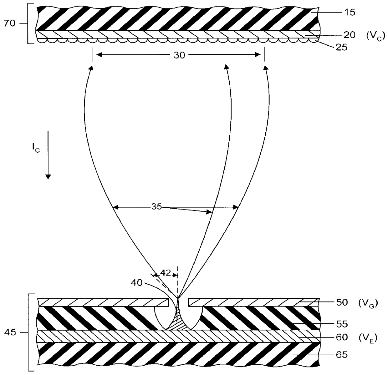
The present invention provides for a process of conditioning newly fabricated FEDs to remove contaminant particles contained therein. The conditioning process is performed before the FED device is used in normal operations, and is typically performed during manufacturing. During the conditioning process of the present invention, contaminants contained in the vacuum tube of an FED are bombarded by a large amount of electrons. As a result of the bombardment, the contaminants will be knocked off and collected by a gas-trapping device (e.g., a getter). Because newly fabricated FEDs contain a large amount of contaminants, precautions steps must be taken to ensure that arcing does not occur during the conditioning process in accordance with the present invention. To this end, according to the present invention, the conditioning process includes the step of driving the anode to a predetermined high voltage and the step of enabling the emission cathode thereafter to ensure that the electron...


PUM


Abstract

A method of removing contaminant particles in newly fabricated field emission displays. According to one embodiment of the present invention, contaminant particles are removed by a conditioning process which includes the steps of: a) driving a anode of a field emission display (FED) to a predetermined voltage; b) slowly increasing an emission current of the FED after the anode has reached the predetermined voltage; and c) providing an ion-trapping device for catching the ions and particles knocked off, or otherwise released, by emitted electrons. In this embodiment, by driving the anode to the predetermined voltage and by slowly increasing the emission current of the FED, contaminant particles are effectively removed without damaging the FED. The present invention also provides a method of operating FEDs to prevent gate-to-emitter current during turn-on and turn-off. In this embodiment, the method comprises the steps of: a) enabling the anode display screen; and, b) enabling the electron-emitters after the anode display screen is enabled. In this embodiment, by allowing sufficient time for the anode display screen to reach a predetermined voltage before the emitter is enabled, the emitted electrons will be attracted to the anode.

Description

The present invention pertains to the field of flat panel display screens. More specifically, the present invention relates to the field of flat panel field emission display screens.Flat panel field emission displays (FEDs), like standard cathode ray tube (CRT) displays, generate light by impinging high energy electrons on a picture element (pixel) of a phosphor screen. The excited phosphor then converts the electron energy into visible light. However, unlike conventional CRT displays which use a single or in some cases three electron beams to scan across the phosphor screen in a raster pattern, FEDs use stationary electron beams for each color element of each pixel. This requires the distance from the electron source to the screen to be very small compared to the distance required for the scanning electron beams of the conventional CRTs. In addition, FEDs consume far less power than CRTs. These factors make FEDs ideal for portable electronic products such as laptop computers, pocke...

Claims


Application Information

Patent Timeline
Patent Type & Authority Patents(United States)
IPC IPC(8): G09G3/22H01J9/44H01J29/04H01J31/12
CPCG09G3/22H01J9/39H01J9/44H01J31/127G09G2310/06G09G2310/066G09G2330/02H01J2209/0223G09G3/20
Inventor ELLOWAY, DONALD J.MORRIS, DAVID L.SCANNELL, WILLIAM J.SPINDT, CHRISTOPHER J.
Owner CANON KK
Why Eureka
Try Eureka