
Method of growing a ZnS:Mn phosphor layer for use in thin-film electroluminescent components

a technology of electroluminescent components and phosphor layers, which is applied in the direction of luminescent compositions, coatings, chemistry apparatuses and processes, etc., can solve the problems of increasing the cost of el display manufacturing process, affecting the performance of electroluminescent zns, and limiting the use of frequency modulation in the generation of different gray levels, etc., to achieve the effect of simplifying the manufacturing process of such thin films and improving the performance of electroluminescent z

Inactive Publication Date: 2000-09-05
PLANAR SYSTEMS +1
View PDF5 Cites 157 Cited by
  • Summary
  • Abstract
  • Description
  • Claims
  • Application Information

AI Technical Summary

Benefits of technology

It is an object of the present invention to overcome the drawbacks of the above-described technique and to provide an entirely novel approach to the growth of manganese-doped zinc sulfide phosphor layers for use in electroluminescent display components. It is a particular object of the invention to improve the performance of electroluminescent ZnS:Mn thin films produced by ALE and to simplify the manufacturing process of such thin films.
The present invention offers significant benefits as compared to both the conventional ALE process for forming electroluminescent ZnS:Mn layers (chloride process) and the use of zinc oxyacetate.
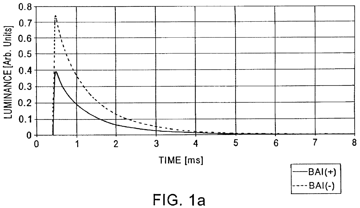
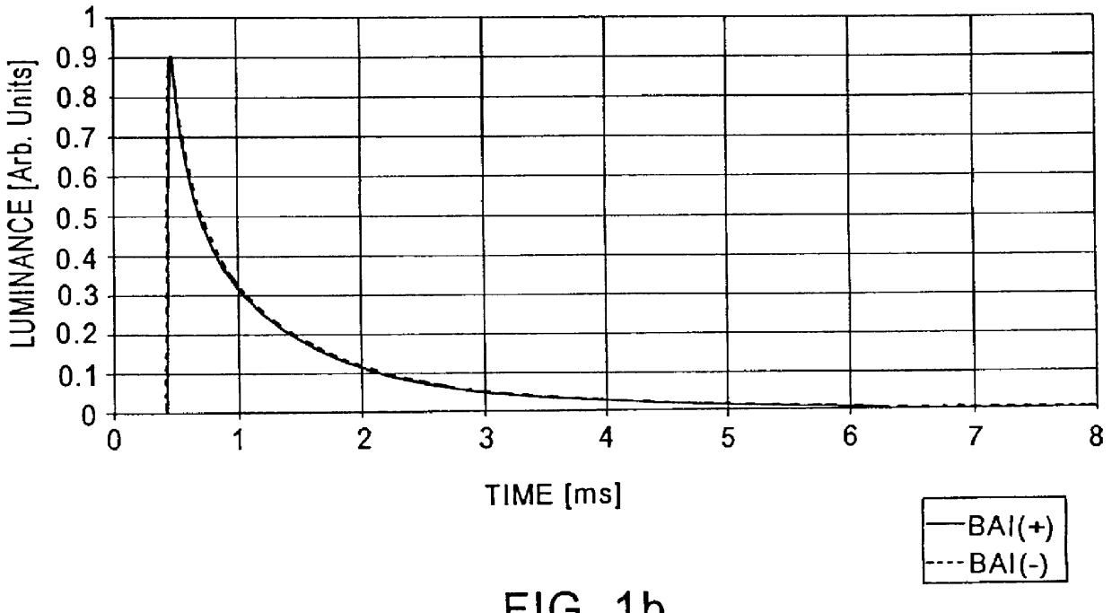
The electroluminescent ZnS:Mn structure according to the invention provides the drive-voltage-symmetrical light emission property which is crucial in the control of gray-scale displays. A comparison of the characteristics plotted for the EL thin-film structure according to the invention prepared in Example 1 and those of the structure prepared according to conventional techniques as exemplified in Examples 1 and 4 makes it evident that the present invention offers a vastly improved and more symmetrical light emission.
The luminance of the display using an electroluminescent ZnS:Mn structure according to the invention degrades at a lower rate and the display exhibits a smaller degree of pattern burning which is due to the lesser rate of luminance degradation of individual pixels during prolonged use.
In the ALE process according to the invention for forming an electroluminescent ZnS:Mn structure, the use of an organic precursor permits the substrate temperature to be kept clearly below the softening point of soda lime glass, whereby economical losses due to warping of the glass substrate are eliminated.

Problems solved by technology

Therefore, it is more difficult in the MOCVD method to achieve good uniformity of the deposited film, which explains why this method has not been used in the large-scale production of electroluminescent ZnS:Mn thin-film components.
However, this conventional technique involves a few evident disadvantages.
In practice, this sets limitations to the use of frequency modulation in the generation of different gray levels on an electroluminescent display, because visible flicker of the emitted light will occur at low drive frequencies due to the asymmetric light emission.
Because soda lime glass is subject to softening already in the temperature range conventionally used, this phenomenon gives rise to extra costs in the manufacturing process of EL displays.
For the handling of both zinc and manganese chloride, the ALE deposition equipment must be provided with sublimation sources which are both clumsy to handle and difficult to control.
Furthermore, as zinc chloride forming the matrix of the thin-film compound is consumed at a higher rate of the two precursors, zinc chloride is obviously the one causing more problems.

Method used


Image

  • Method of growing a ZnS:Mn phosphor layer for use in thin-film electroluminescent components
  • Method of growing a ZnS:Mn phosphor layer for use in thin-film electroluminescent components
  • Method of growing a ZnS:Mn phosphor layer for use in thin-film electroluminescent components

Examples


example 1

Growth of ZnS:Mn phosphor for TFEL components by ALE using hydrogen sulfide, diethylzinc and Mn(thd).sub.3 as precursors and respectively hydrogen sulfide and chlorides as precursors in a comparative process.

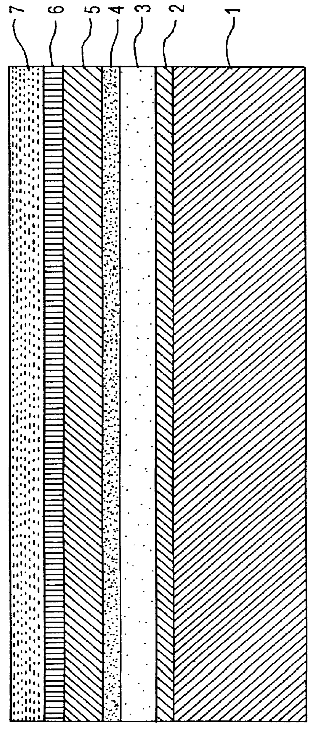
The thin-film structure of the TFEL component prepared in the example is shown in FIG. 2. Referring to the diagram, the phosphor layer of the TFEL component is grown on a soda lime glass substrate 1, on the surface of which is first made an Al.sub.2 O.sub.3 ion-diffusion barrier layer 2 and an ITO conductor pattern 3. By ALE, on the ITO conductor layer is grown an Al.sub.x Ti.sub.y O.sub.z compound oxide insulation layer 4 using aluminum chloride, titanium chloride and water as reagents. A ZnS:Mn phosphor layer 5 is next grown by two different methods: A) using hydrogen sulfide, pulverized zinc chloride and MnCl.sub.2 as reagents at 510.degree. C. growth process temperature and B) using hydrogen sulfide, liquid diethylzinc and Mn(thd).sub.3 as reagents at 350.degree. C. growth p...

example 2

Growth of ZnS:Mn phosphor for TFEL components by ALE using hydrogen sulfide, diethylzinc and bis(cyclopentadienyl) manganese Mn(cpd).sub.2 as precursors.

In this process, the phosphor layer of a TFEL component is grown on a soda lime glass substrate having its surface covered with an Al.sub.2 O.sub.3 ion-diffusion barrier layer and an ITO conductor pattern. On the ITO conductor pattern is grown by ALE an Al.sub.x Ti.sub.y O.sub.z compound oxide insulation layer in the same manner as described in Example 1 above using aluminum chloride, titanium chloride and water as reagents. The zinc sulfide matrix of the phosphor layer is grown at 350.degree. C. substrate surface temperature using liquid diethylzinc and hydrogen sulfide as precursors. Doping with manganese is accomplished by sequentially pulsed infeed of Mn(cpd).sub.2 and hydrogen sulfide. Zinc sulfide is deposited for 100 cycles, whereby the surface of the glass substrate is subjected to a train of reagent pulses 100.times.(diethy...

example 3

Growth of ZnS:Mn phosphor for TFEL components by ALE using t-butylmercaptan, dimethylzinc and bis(methylcyclopentadienyl) manganese (BCPM) as precursors.

In this process, the phosphor layer of a TFEL component is grown on a soda lime glass substrate having its surface covered with an Al.sub.2 O.sub.3 ion-diffusion barrier layer and an ITO conductor pattern. On the ITO conductor pattern is grown by ALE an Al.sub.x Ti.sub.y O.sub.z compound oxide insulation layer in the same manner as described in Examples 1 and 2 above using aluminum chloride, titanium chloride and water as reagents. The zinc sulfide matrix of the phosphor layer is grown at 300.degree. C. substrate temperature using liquid dimethylzinc and t-butyl mercaptan as precursors. Doping with manganese is accomplished by sequentially pulsed infeed of bis(methylcyclopentadienyl) manganese and hydrogen sulfide. Zinc sulfide is deposited for 100 cycles, whereby the surface of the glass substrate is subjected to a train of reagent...


PUM

PropertyMeasurementUnit
temperatureaaaaaaaaaa
pressureaaaaaaaaaa

Abstract

The invention relates to a method of growing a ZnS:Mn phosphor layer suitable for use in thin-film electroluminescent components. According to the method, the ZnS:Mn phosphor layer is grown on a substrate by means of the ALE method using volatile zinc, sulfur and manganese compounds as the precursors. According to the invention, an organozinc compound such as diethylzinc or dimethylzinc is used as precursor for zinc, hydrogen sulfide or an organosulfur compound is used as precursor for sulfur, and an organomanganese compound or organic manganese complex compound is used as precursor for manganese. The invention provides a display component with drive-voltage-symmetrical light emission and stable characteristics of luminance level and turn-on voltage.

Description

1. Field of the InventionThe present invention relates to the manufacture of thin-film components. In particular, the present invention concerns a method for growing a ZnS:Mn phosphor layer for use in inorganic thin-film electroluminescent components, wherein the ZnS:Mn phosphor layer is grown on a substrate by means of the Atomic Layer Epitaxy method. According to the method, volatile (i.e., gaseous or vaporizable) zinc, sulfur and manganese compounds are used as precursors for preparing the layer to be deposited.2. Description of Related ArtFlat electroluminescent displays are used in applications requiring a wide viewing angle, a wide temperature range and a rugged device structure. The most important electroluminescent phosphor material is manganese-doped zinc sulfide (ZnS:Mn) which is conventionally used in all monochrome electroluminescent displays emitting yellow light. Also polychrome electroluminescent displays emitting red and green are based on the same phosphor material,...

Claims


Application Information

Patent Timeline
Patent Type & Authority Patents(United States)
IPC IPC(8): C09K11/57H05B33/10H05B33/14H05B33/12C09K11/56
CPCC09K11/574H05B33/10H05B33/12H05B33/14
Inventor SOININEN, ERKKI LAURIHARKONEN, GITTELAHONEN, MARJATORNQVIST, RUNARVILJANEN, JUHA
Owner PLANAR SYSTEMS
Learn More