Etch process for forming high aspect ratio trenched in silicon

a technology of high aspect ratio and etch process, which is applied in the direction of surface treatment compositions, chemistry apparatus and processes, transistors, etc., can solve the problems of reducing the throughput of single substrate processing, limiting the use of etchant compositions, and adding to the cost of making these semiconductor devices

Inactive Publication Date: 2000-10-03
APPLIED MATERIALS INC
View PDF20 Cites 114 Cited by
  • Summary
  • Abstract
  • Description
  • Claims
  • Application Information

AI Technical Summary

Problems solved by technology

Conventional etchant compositions such as HBr and oxygen can form such devices, but there are limitations in the use of this etchant composition.
Since particles are highly undesirable because they can fall onto the substrates being processed in the chamber, the chamber must be cleaned often, generally after each substrate is processed.
The need for such frequent cleaning reduces the throughput of single substrate processing, and adds to the cost of making these semiconductor devices.
Various halogen-containing etchants for silicon-containing materials are known, but all of them have various characteristics that make them inadequate as etchants for making small diameter, deep openings having straight walls in silicon.
Some etchants etch isotropically rather than anisotropically; some etchants deposit polymer-containing materials on the sidewalls of the trench, preventing smooth filling of the trench; some produce bowed or shaped sidewalls that cannot be filled properly; some of them have low etch rates; and some of them require high chamber power that causes damage to or contamination of the substrate.
Microloa

Method used


Image

  • Etch process for forming high aspect ratio trenched in silicon
  • Etch process for forming high aspect ratio trenched in silicon
  • Etch process for forming high aspect ratio trenched in silicon

Examples


example 2

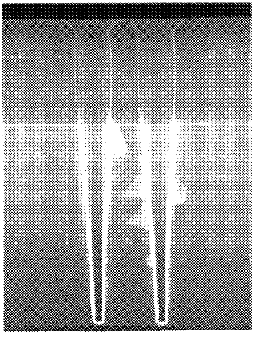
The procedure of Example 1 was followed, except that an aqueous 100:1 water:HF dip was used after step 2 to remove the passivation layer, as shown in FIG. 10.

example 3

This example illustrates that the profile angle can be controlled using the present two step process. The procedure of Example 1 was followed, except that in the second etch step, 800 watts of power was connected to the coil.

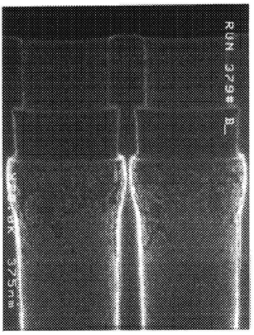
In Part A, the second etch step etchant used was 45 sccm SF.sub.6, 52 sccm HBr and 47 sccm O.sub.2. As shown in FIG. 11, the angle at the top of the trench was 89.2.degree. and the angle at the bottom was 90.5.degree.. There is a clear demarcation between the two etchants and the bottom of the trench is tapered outwardly, and is thus wider than the top of the trench.

In Part B, the second etch step used 45 sccm SF.sub.6, 80 sccm HBr and 47 sccm O.sub.2. The top of the trench had an angle of 88.5.degree., about perpendicular. As shown in FIG. 12, this produced a trench having a slightly tapered opening at the top.

In Part C, the second etch used was 45 sccm SF.sub.6, 100 sccm HBr and 47 sccm O.sub.2. The top of the trench had an angle of 88.2.degree. and the bottom...


PUM

PropertyMeasurementUnit
Pressureaaaaaaaaaa
Pressureaaaaaaaaaa
Poweraaaaaaaaaa

Abstract

A multistep etch process for forming high aspect ratio trenches in silicon having a silicon oxide and/or silicon nitride hardmask. In a first step, an etch composition of HBr and oxygen is used, depositing a passivation layer on the sidewalls and producing slightly tapered openings. In the second step, an etch composition of a fluorine-containing gas such as SF6, HBr and oxygen is used, producing more vertical openings at a high etch rate. The taper of the openings during the second step can be controlled by adjusting the relative amount of HBr or SF6 employed. This process is a clean process that does not require cleaning of the etch chamber between etch steps.

Description

This invention relates to a new etch process for etching high aspect ratio openings in silicon. More particularly, this invention relates to a new etch process for etching very small diameter openings in silicon, i.e., a diameter less than 0.25 micron.BACKGROUND OF THE DISCLOSUREAs devices for the semiconductor industry have become smaller and more closely packed together, processes to make such devices must be developed. In order to make devices such as DRAMS, high aspect ratio, straight walled trenches need to be made in silicon which are then filled with one or more dielectric layers to form capacitors. The trenches must be completely filled without voids.In order to make 256 MB devices, openings in silicon must be etched that have a diameter on the order of 0.25-0.3 micron that are at least 8 microns deep. Conventional etchant compositions such as HBr and oxygen can form such devices, but there are limitations in the use of this etchant composition. As etching continues, the etc...

Claims


Application Information

Patent Timeline
IPC IPC(8): H01L21/02H01L21/3065H01L21/302H01L21/8242H01L27/108
CPCH01L21/3065
Inventor WANG, YIQIONGLI, MAOCHENGPAN, SHAOHER
Owner APPLIED MATERIALS INC
Why Eureka
Try Eureka