Method for depositing fine-grained alumina coatings on cutting tools

a technology of alumina coating and cutting tool, which is applied in the direction of manufacturing tools, turning machine accessories, other chemical processes, etc., can solve the problems of excessive cracking of coating, electrical breakdown and arcing, and affecting both the growth rate and the quality of coating in a detrimental way

Inactive Publication Date: 2000-10-31
SANDVIK INTELLECTUAL PROPERTY AB
View PDF8 Cites 36 Cited by
  • Summary
  • Abstract
  • Description
  • Claims
  • Application Information

AI Technical Summary

Problems solved by technology

The tensile stresses may exceed the rupture limit of Al.sub.2 O.sub.3 and cause the coating to crack extensively and a network of cooling cracks will be generated over the entire Al.sub.2 O.sub.3 layer.
However, certain problems arise when employing these plasma-based techniques for the deposition of highly insulating layers such as Al.sub.2 O.sub.3.
Furthermore, these insulating layers will become charged which may cause electrical breakdown and arcing.
This latter phenomenon naturally effects both the growth rate and the quality of the coating in a detrimental way.
The PVD techniques in general have, due to the low process pressure, the disadvantage of being so-called "line of sight" methods, i.e., only surfaces facing the ion source will be coated.
A disadvantage with the DC voltage generation of plasmas, including the unipolar pulsed DC voltage technique, is that the surface charging on the nonconducting layers cannot totally be suppressed.
Specifically, the charging is most severe on sharp corners and along edges of the substrates resulting in a significant decrease in the layer thickness and also in the quality of the coating.
In more general terms, the fact that the insulating alumina layer grows not only on the substrates but equally on all surfaces in the vicinity, the plasma as well as on the electrodes, will negatively influence the stability of the plasma and the entire deposition process may eventually end in the extinction of the discharge.
By not allowing the voltage to attain zero potential may have a preferable effect on the deposition rate but simultaneously results in a more severe charge built-up on non-conducting surfaces.

Method used


Image

  • Method for depositing fine-grained alumina coatings on cutting tools
  • Method for depositing fine-grained alumina coatings on cutting tools
  • Method for depositing fine-grained alumina coatings on cutting tools

Examples


example 1

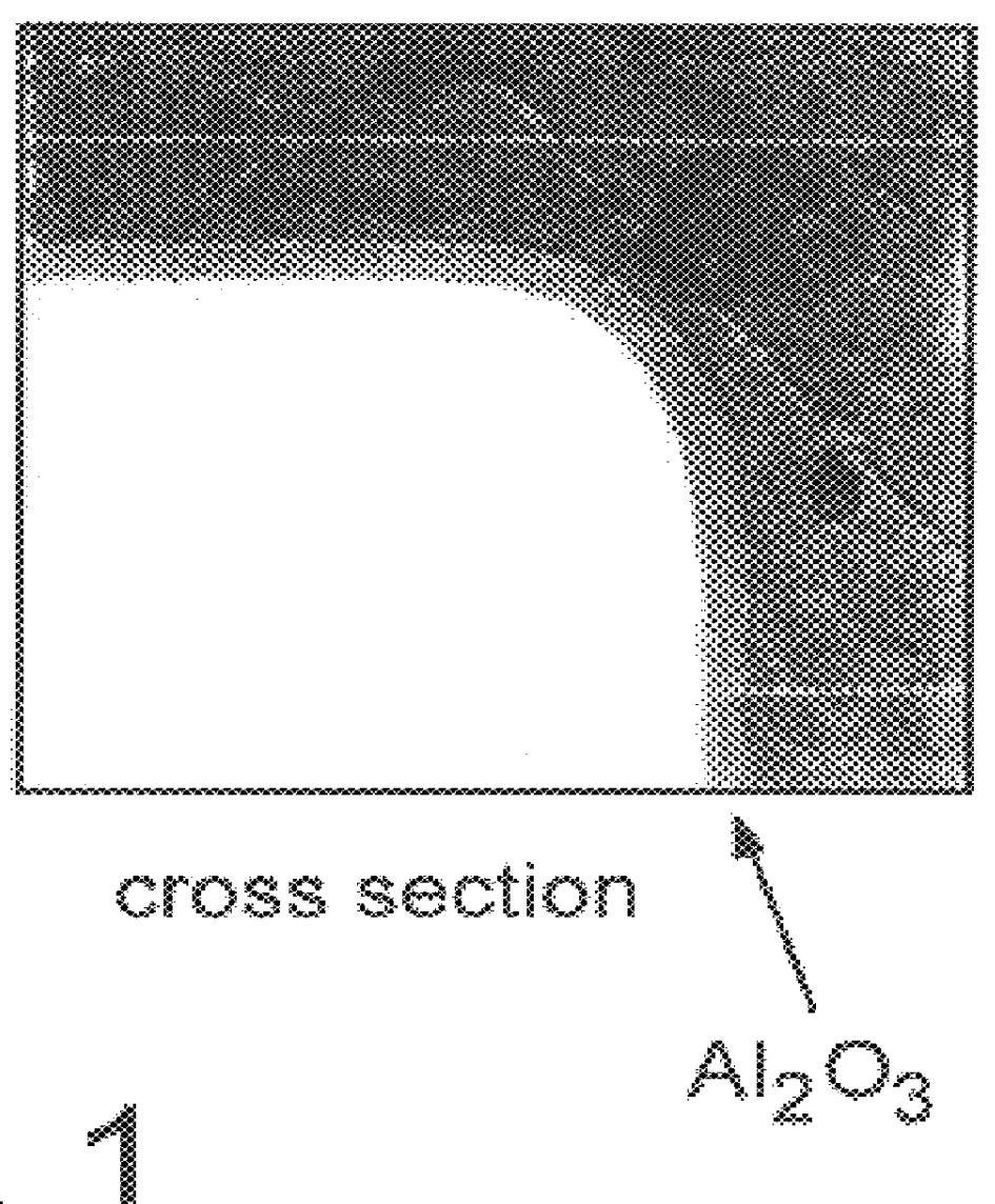
A) Cemented carbide inserts of style CNMA 120412-KR having a composition of 6 w % Co and balance WC were coated with a first layer of 6 .mu.m TiCN and thereafter with a top layer of 1.5 .mu.m .kappa.-Al.sub.2 O.sub.3. Both the TiCN and the Al.sub.2 O.sub.3 layer were deposited by conventional CVD technique. The Al.sub.2 O.sub.3 layer had an average grain size of 1 .mu.m.

B) Cemented carbide inserts of the same style and composition as in A were first coated with an approximately 2.5 .mu.m TiN layer by an ion plating technique.

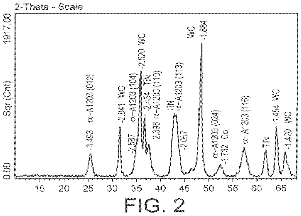
C) Inserts from B were coated with 5.3 .mu.m fine-grained .alpha.-Al.sub.2 O.sub.3 layer in a separate experiment with the bipolar pulsed DC voltage PACVD technique under the conditions given below:

D) Inserts from B were coated with 5.9 .mu.m fine-grained .gamma.-Al.sub.2 O.sub.3 layer in a separate experiment with the bipolar pulsed DC voltage PACVD technique under the conditions given below:

X-ray diffraction (XRD) analysis when using Cu.sub..kappa..alpha. radi...

example 2

E) Cemented carbide inserts of style CNMA 120412-KR having a composition of 6 w % Co and balance WC were coated with a first layer of approximately 2.5 .mu.m TiN by an ion plating technique and thereafter coated with a 3 .mu.m fine-grained Al.sub.2 O.sub.3 layer in a separate experiment with the bipolar pulsed DC voltage PACVD technique under the following deposition conditions:

XRD analysis (FIG. 7) showed a broad peak at the 2.theta. angle 66.8.degree. corresponding to the (440) planes of .gamma.-Al.sub.2 O.sub.3. The broad XRD peak indicates a very fine-grained .gamma.-Al.sub.2 O.sub.3. The microhardness HV(0.02) of the coating was determined to 19 GPa. A chlorine concentration of 1.5 at % was determined. The coating appeared fully transparent.

example 3

F) Cemented carbide inserts of style CNMA 120412-KR having a composition of 6 w % Co and balance WC were coated with a first layer of approximately 2.5 .mu.m TiN layer by an ion plating technique and thereafter coated with a 2.5 .mu.m fine-grained Al.sub.2 O.sub.3 layer in a separate experiment with the bipolar pulsed DC voltage PACVD technique under the following deposition conditions:

XRD analysis (FIG. 8) showed a distinct peak at the 2.theta.-angle 66.8.degree. corresponding to the (440) planes of .gamma.-Al.sub.2 O.sub.3. The microhardness HV(0.02) was determined to 22 GPa.


PUM

PropertyMeasurementUnit
temperatureaaaaaaaaaa
total process pressureaaaaaaaaaa

Abstract

A method for depositing refractory alumina (A2O3) thin layers on cutting tools made of cemented carbide, cermet, ceramics or high speed steel is disclosed. The present method is a Plasma Activated Chemical Vapor Deposition (PACVD) process in which the plasma is produced by applying a bipolar pulsed DC voltage across two electrodes to which the tool substrates to be coated are fixtured and electrically connected. In contrast to prior art methods, built-up electrical charge on non-conducting surfaces is suppressed and hence, no arcing occurs on said surfaces. This will permit stable, long-term processing, With the present method, high-quality coatings of either single phase gamma-Al2O3 or of a mixture of gamma- and alpha-Al2O3 phases can be deposited on cutting tools at deposition temperatures as low as 500 DEG C. When coated cemented carbide tools according to the invention are used in the machining of steel or cast iron, several important improvements to prior art produced Al2O3-coated tools have been observed.

Description

The present invention relates to a method for depositing fine-grained, crystalline Al.sub.2 O.sub.3 (alumina) coatings on cutting tools having a body of cemented carbide, cermet, ceramics or high speed steel by means of a Plasma Activated Chemical Vapor Deposition (PACVD) process with the chemical reactants AlCl.sub.3, O.sub.2, H.sub.2 and Ar. The plasma is produced by applying a bipolar pulsed DC voltage on two electrodes or two sets of electrodes. It is possible, with the present method, to deposit at high deposition rate, smooth, high-quality coatings consisting of either single phase gamma-Al.sub.2 O.sub.3 or of a mixture of gamma- and alpha-Al.sub.2 O.sub.3 phases. The coatings have a good wear resistance when applied on cutting tools. With the present method, crystalline Al.sub.2 O.sub.3 coatings can be obtained at deposition temperatures as low as 500.degree. C. The present method, bipolar pulsed DC voltage PACVD, can also successfully be used for the deposition of non-insula...

Claims


Application Information

Patent Timeline
Patent Type & Authority Patents(United States)
IPC IPC(8): C23C16/40C23C16/515C23C16/50B23P15/28C23C16/12B23B27/14C23C16/503C23C16/513
CPCC23C16/515C23C16/403B23B27/148B23B2228/04
Inventor TASCHNER, CHRISTINEENDLER, INGOLFLEONHARDT, ALBRECHTLJUNGBERG, BJORNSJOSTRAND, MATS
Owner SANDVIK INTELLECTUAL PROPERTY AB
Why Eureka
Try Eureka