

Method for manufacturing a semiconductor device
a manufacturing method and semiconductor technology, applied in semiconductor/solid-state device manufacturing, basic electric elements, electric devices, etc., can solve the problems of inferior electrical characteristics of amorphous silicon and crystalline silicon, and the problem of not being completely solved
- Summary
- Abstract
- Description
- Claims
- Application Information
AI Technical Summary
Problems solved by technology
Method used
Image

Examples
example 1
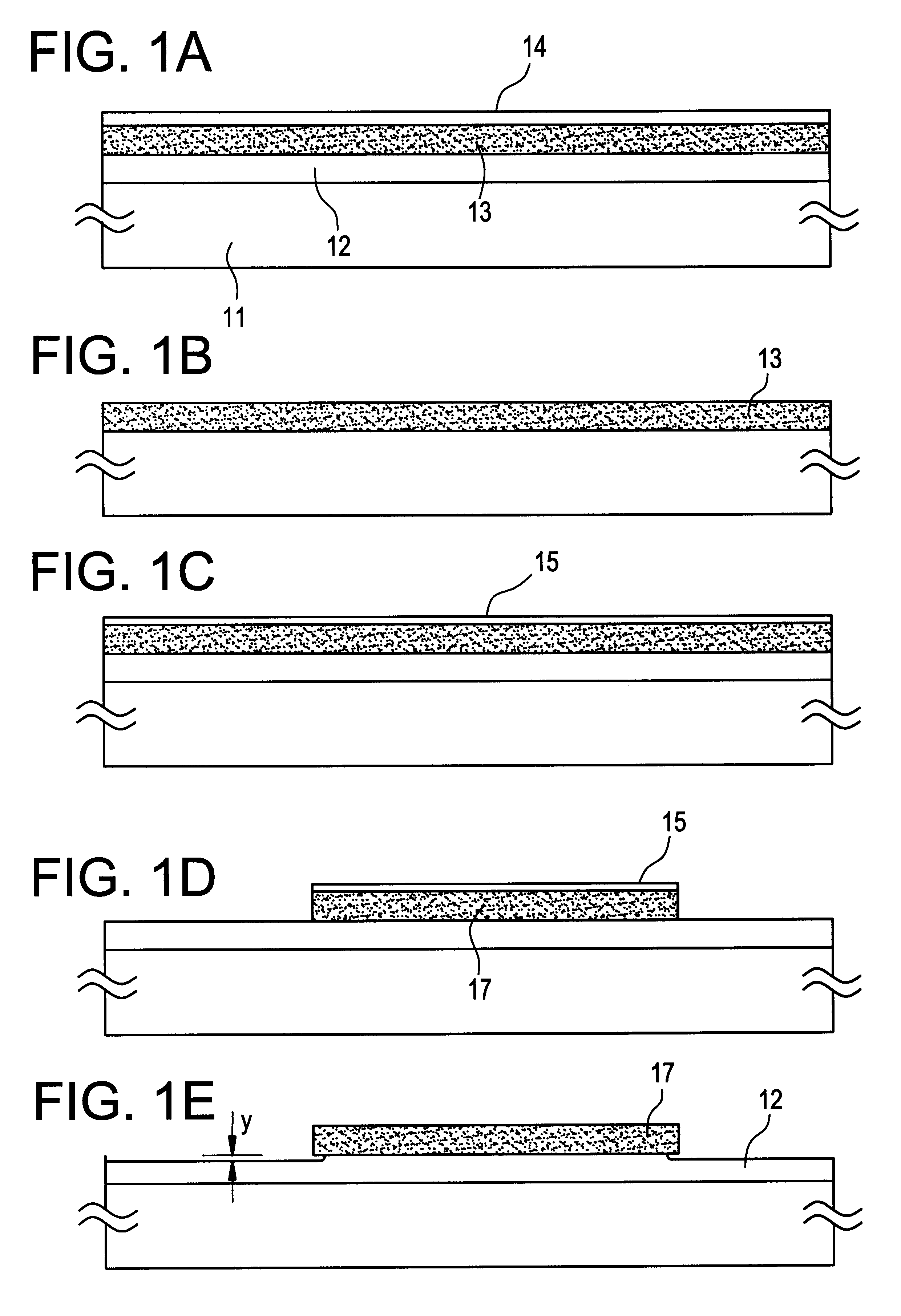
FIGS. 1A through 1E show cross sectional views of a manufacturing process in accordance with the first example of the present invention.
Initially, a silicon oxide film 12 is formed on a substrate 11 (Corning 7059) by sputtering to a thickness of 2000 .ANG.. It is preferable to heat the substrate prior to or after the formation of the silicon oxide film 12 at a temperature higher than a strain point of the substrate and then cool it below the strain point at a cooling rate of 0.1-1.0.degree. C. / minute. This treatment suppresses the contraction of the substrate due to subsequent heating steps (including the oxidation process of the invention with IR radiation or heat annealing), making a mask aligning process easier. In the case of the Corning 7059 like in this example, the substrate is heated at a temperature 620.degree.-660.degree. C. for 1 to 4 hours then cooled to 450-590.degree. C. at cooling rate of 0.1-1.0.degree. C., preferably 0.1-0.3.degree. C., at which temperature the subs...
example 2
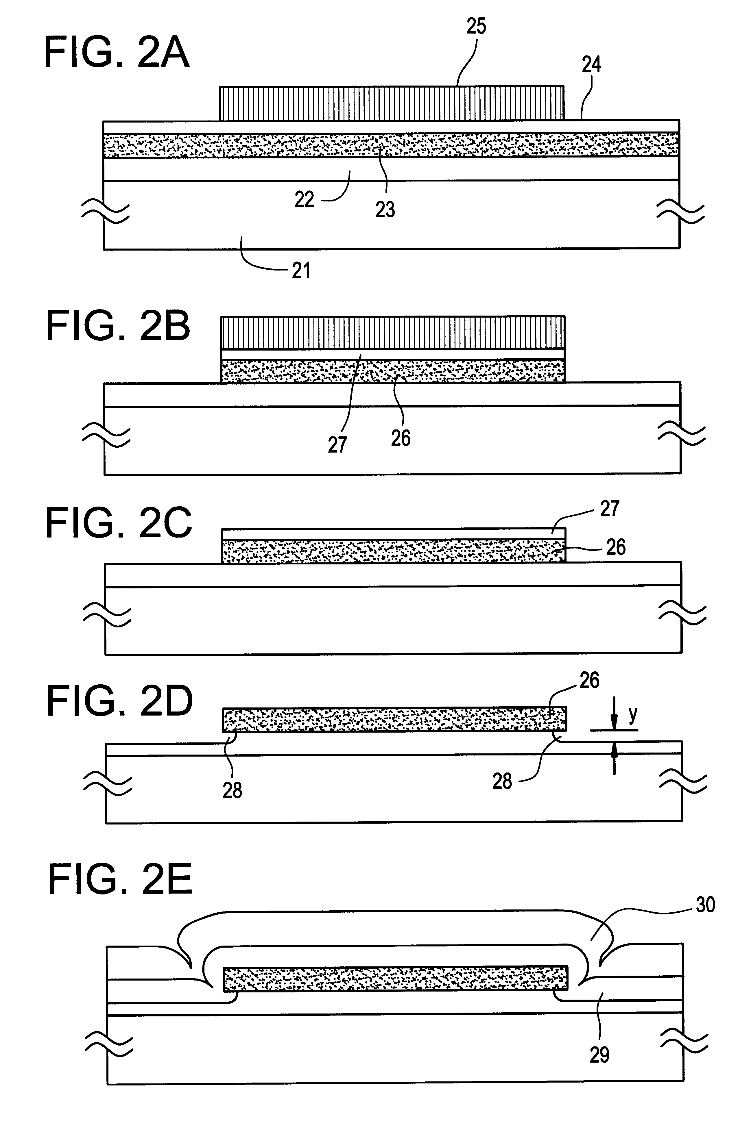
The process in the second example of this invention will be described in conjunction with FIGS. 3A-3E. A Corning 7059 glass substrate (1.1 mm thick, 300 mm.times.400 mm) is used as a substrate 31. In the same manner as in the first example, the substrate is initially heated at 640.degree. C. for one hour and then cooled to 580.degree. C. at a cooling rate of 0.2.degree. C. / minute. A silicon oxide is deposited on the substrate 31 as a blocking layer 32 to a thickness of 2000 .ANG. by a plasma CVD. TEOS is used as a precursor gas and the substrate is maintained at 350.degree. C.
Then, an amorphus silicon layer 33 is formed to a thickness of 500 .ANG. by a LPCVD or plasma CVD on the blocking layer 32. Further, a silicon oxide layer 34 having a thickness of 1000 .ANG. is provided on the amorphous silicon layer 33 through a plasma CVD, following which a portion of the amorphous silicon 33 is exposed by patterning the silicon oxide layer by a known photolithography. Then, a thin nickel fil...
example 3
The process of the third example of this invention will be described in conjunction with FIGS. 4A to 4E. The same substrate 41 having a silicon oxide layer 42 and an amorphous silicon layer 43 is prepared in the same manner as in the previous examples.
On the amorphous silicon film 43, a photoresist layer 44 is provided by spin coating to a thickness of 2 .mu.m, following which the photoresist layer is patterned by a known photolithography in order to expose a portion of the silicon layer. Further, a nickel film 45 of a thickness 10 .ANG.or less is formed by a sputtering method. (FIG. 4A)
Then, as shown in FIG. 4B, the photoresist layer 44 is removed by a known process while the nickel film directly formed on the portion of the silicon layer (as designated with a reference numeral 46) remains unremoved.
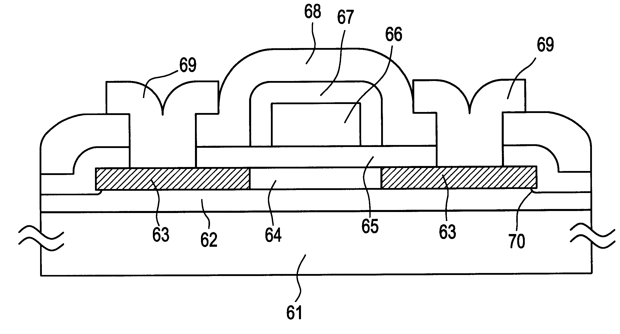
Then, the substrate is heated at 550.degree. C. for 8 hours, or at 600.degree. C. for 4 hours in a nitrogen gas. As a result, the silicon layer is crystallized in a direction shown by t...
PUM
 Abstract
Description
Claims
Application Information