Rapid and accurate end point detection in a noisy environment

a technology of end point detection and noisy environment, which is applied in the direction of manufacturing tools, lapping machines, instruments, etc., can solve the problems of inability to accurately measure film thickness, distortion or noise in the light 10 of the light, and the inability to monitor film thickness in situ

Inactive Publication Date: 2001-01-09
FILMETRICS
View PDF20 Cites 183 Cited by
  • Summary
  • Abstract
  • Description
  • Claims
  • Application Information

AI Technical Summary

Problems solved by technology

A problem with such methods as applied to CMP is that the monitoring of the film thickness cannot typically be done in in situ, i.e., while chemical mechanical planarization of the wafer is underway.
The reason is that the slurry introduces a distortion into the reflected light, making it difficult if not impossible to accurately measure film thickness.
This process introduces distortion or noise into the light 10.
Since monitoring of film thickness must be performed periodically if not continuously, the overhead involved in repeatedly stopping the CMP procedure, and removing the slurry, can be prohibitively expensive in terms of reduced throughput of the CMP procedure.
In many cases, this renders the optical method of film measurement infeasible for application to CMP because of the overhead involved.
Another problem with such approaches is that distortion introduced by the optical components of the film measuring apparatus can adversely impact the accuracy of film thickness measurement.
However, such methods are computationally complex, require time-consuming comparisons with theoretical or expected waveforms, employ excessive numbers of analytical steps to determine film thickness, or require time-consuming angular and mechanical movements or sweeps of an optical device such as a mirror.
Consequently, in many cases, the process of monitoring film thickness employing such methods cannot be performed in real time, i.e., concurrently with and without requiring stoppage of CMP processing.
The result is a reduced throughput of CMP processing.

Method used


Image

  • Rapid and accurate end point detection in a noisy environment
  • Rapid and accurate end point detection in a noisy environment
  • Rapid and accurate end point detection in a noisy environment

Examples


first embodiment

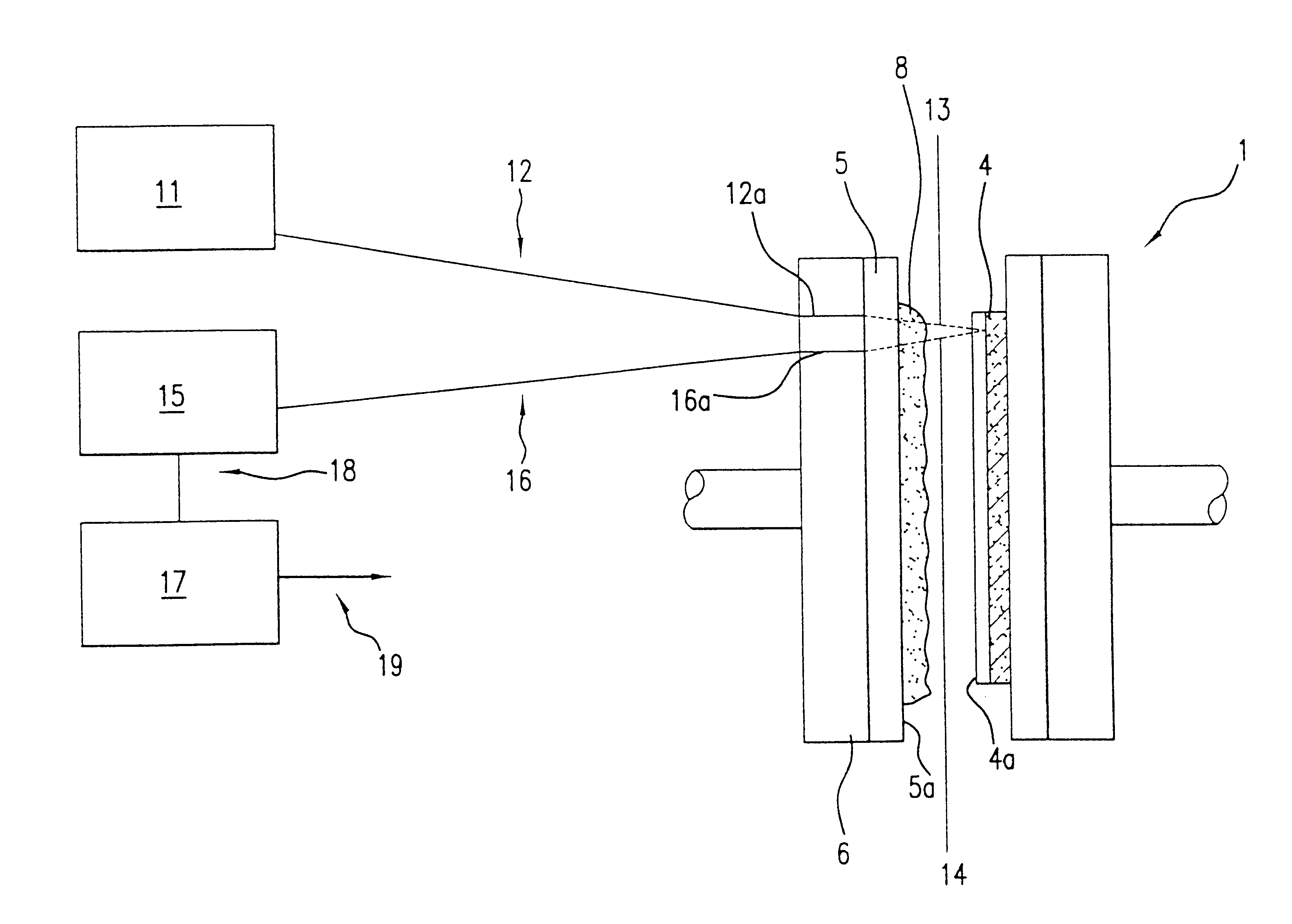
the subject invention, suitable for use in measuring the thickness of transparent or semi-transparent films, is illustrated in FIG. 3, in which, compared to FIGS. 1-2, like elements are referenced with like identifying numerals. Advantageously, the film to be measured ranges in thickness from 0.0001 .mu.m. to 500 .mu.m., but it should be appreciated that this range is provided by way of example only, and not by way of limitation. This embodiment is advantageously configured for use with CMP station 1, previously illustrated in FIGS. 1-2. This embodiment also comprises a light source 11 coupled to an optical fiber or fiber bundle 12 for delivering light from the light source to the CMP station 1. Preferably, the light source is a white light source. Advantageously, the light source is a tungsten-halogen lamp or the like in which the output is regulated so that it is substantially invariant over time.

Also included are fiber / fiber bundle 16, spectrometer 15, and computer 15. Light from...

second embodiment

the subject invention, suitable for performing endpoint detection for opaque films comprised of a material such as metal situated on top of a transparent or semi-transparent substrate, will now be described. This embodiment is similar to the previous embodiment, and is best described in terms of the differences from that embodiment.

According to this embodiment, a precise quantitative measurement of the thickness of the opaque film is not provided. Instead, an endpoint parameter is provided from which an endpoint condition can be detected, i.e., the condition in which the opaque film is or is about to be completely removed from the surface of the transparent / semi-transparent substrate.

This embodiment is particularly well-suited for those applications in which a metal layer is placed over a substrate formed of a material such as an insulator in order to fill contact holes for providing electrical contact to layers below the insulator, and then, in a subtractive process, removed from t...

third embodiment

the subject invention, appropriate for use with patterned films, i.e., films of different thicknesses arranged over a substrate, including but not limited to semiconductor patterned wafers, will now be described. This embodiment is similar to the first embodiment, and so, as with the second embodiment, is best described in terms of its differences from the first embodiment.

This embodiment, as with the first embodiment, is particularly well-suited for use in combination with CMP station 1. In this application, a patterned semiconductor wafer would be positioned on the station in the place of film 4a and substrate 4. However, it should be appreciated that this embodiment can be used to measure patterned films in a variety of other applications, such as the applications discussed involving the placement of anti-reflective coatings on eyewear and automotive plastics, and polyimide coatings on flat panel displays.

With reference to FIG. 15, a patterned semiconductor wafer is illustrated. ...


PUM


Abstract

Methods and apparatus for film measurement and endpoint detection in a noisy environment, such as CMP processing of semiconductor wafers, are disclosed, characterized by the use of spectral analysis of intensity data derived from light reflected off the sample to estimate film thickness or detect an endpoint condition.

Description

I. BACKGROUND OF THE INVENTIONThis invention relates generally to the field of film thickness measurement and film etching and deposition end point detection, and more specifically, to the field of film measurement and end point detection in a noisy environment, such as CMP processing of semiconductor wafers.Many industrial processes require precise control of film thickness. In semiconductor processing, for example, a semiconductor wafer is fabricated in which one or more layers of material from the group comprising metals, metal oxides, insulators, silicon dioxide (SiO.sub.2), silicon nitride (SiN), polysilicon or the like, are stacked on top of one another over a substrate, made of a material such as silicon. Often, these layers are added through a subtractive process in which a layer having a thickness greater than the desired thickness is added to the previous layer, and then polished or ground down to the desired thickness through a process known as chemical mechanical planari...

Claims


Application Information

Patent Timeline
Patent Type & Authority Patents(United States)
IPC IPC(8): B24B49/12B24B37/04B24B49/02G01B11/06B24B37/013
CPCB24B37/013B24B49/02B24B49/12G01B11/0683
Inventor CHALMERS, SCOTT A.GEELS, RANDALL S.
Owner FILMETRICS
Why Eureka
Try Eureka