Analog memory IC with fully differential signal path
a technology of analog memory and signal path, applied in the field of analog memory ic, can solve the problem that the sense amplifier generally consumes power
Inactive Publication Date: 2001-02-06
SANDISK CORP
View PDF17 Cites 40 Cited by
- Summary
- Abstract
- Description
- Claims
- Application Information
AI Technical Summary
Benefits of technology
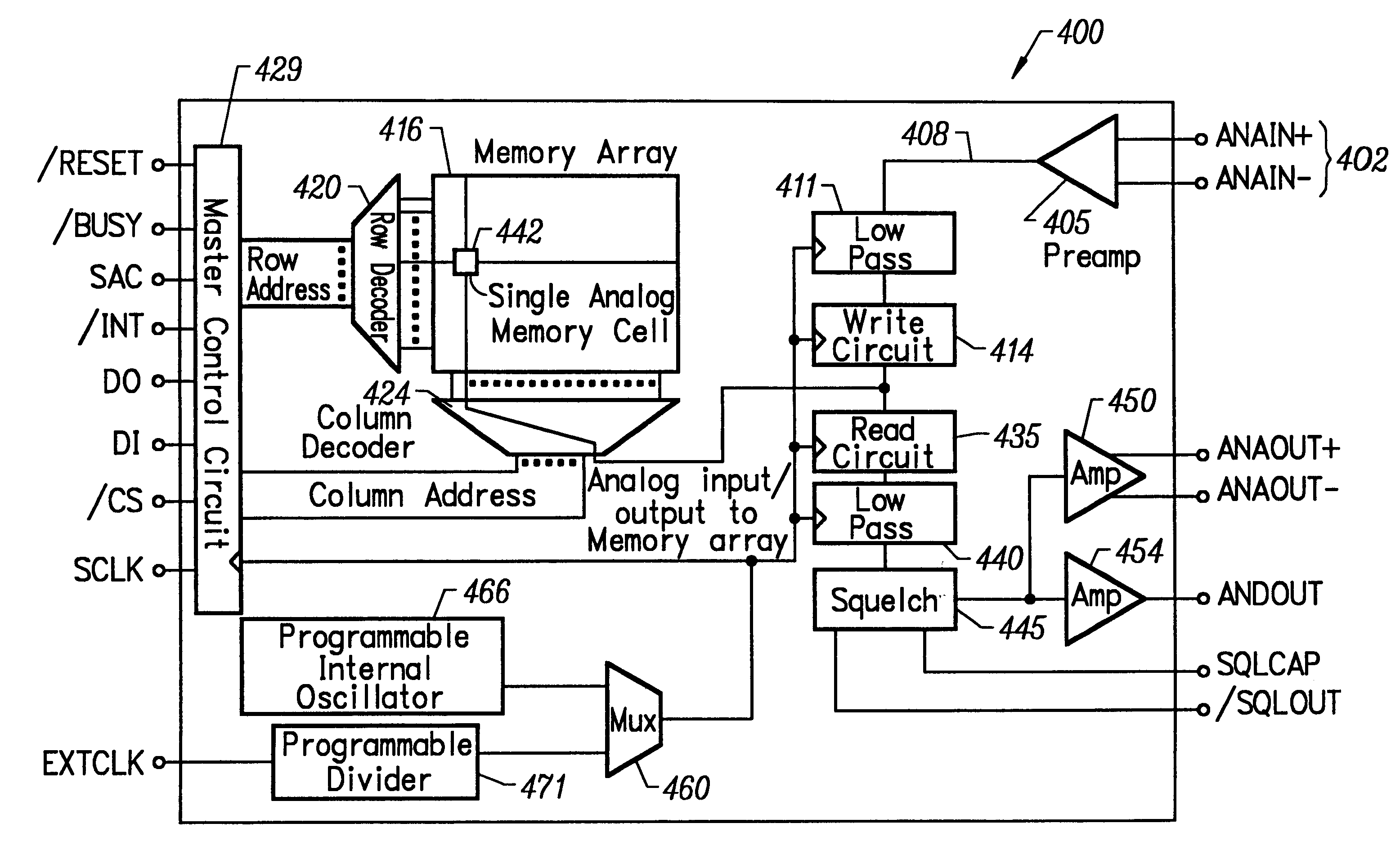
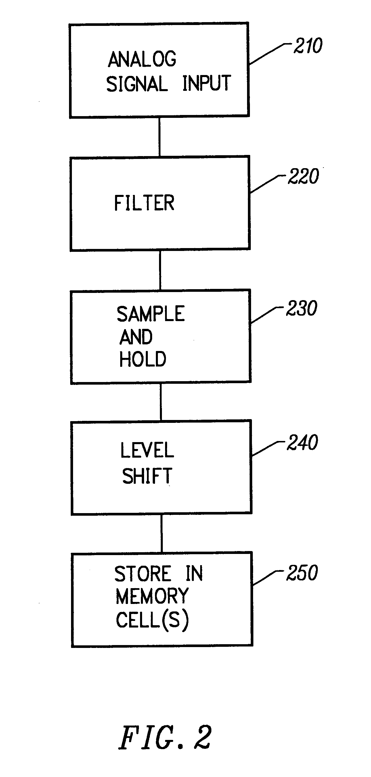
The integrated circuit memory has an internal signal path that is differential. This enhances the precision with which the signal is stored in the memory cells. Among other advantages a fully differential signal pass has inherently an improved common-mode noise rejection. Furthermore, the dynamic range is doubled which may lead to a higher signal to noise ratio and is suitable for low voltage applications. To store analog information the analog input to the integrated circuit has a positive (+) and negative (-) input. The analog input is connected to a preamplifier to amplify the input signal. The preamplifier is fully differential and has a positive and negative output. The preamplifier output is connected to a low pass filter. The filter has positive and negative outputs. These positive and negative outputs are connected to level shifter circuitry. The level shifter performs a sample and hold operation, an amplification, a voltage shift, and a differential to single ended conversion.
The integrated circuit has a master-slave biasing scheme. A master bias generator generates a master bias voltage that is connected to a number of slave bias generators. This master bias voltage may be based on a bandgap voltage reference. The slave bias generators use the master bias voltage to generate a number of slave bias voltages. These slave bias voltages are connected to the various components of the integrated circuit. This scheme of connecting different slave bias generators to different components improve the isolation of the bias voltages among the components. It is less likely that components which couple noise into its slave bias generator will affect the other components connected to different slave bias generators. Also, if a component of the integrated circuit is not being used, its slave bias generator can be disabled to save power.
The integrated circuit has a squelch circuit to attenuate its output signal when an input to the squelch circuit is below threshold level. The squelch circuit essentially greatly attenuates background noise. In effect, there will be a greater signal to noise ratio at the output of the integrated circuit.
Problems solved by technology
A sense amplifier generally consumes power while the sense amplifier is actively sensing.
Method used
View moreImage
Smart ImageViewing Examples
Examples
Embodiment Construction
has been presented for the purposes of illustration and description. It is not intended to be exhaustive or to limit the invention to the precise form described, and many modifications and variations are possible in light of the teaching above. The embodiments were chosen and described in order to best explain the principles of the invention and its practical applications. This detailed description will enable others skilled in the art to best utilize and practice the invention in various embodiments and with various modifications as are suited to the particular use contemplated. The scope of the invention is defined by the following claims.
Login to View More PUM
 Abstract
An integrated circuit memory is capable of storing analog information without the need for A / D conversion. Samples of a analog signal input are stored in nonvolatile memory cells. The integrated circuit is also capable of storing digital information in digital form. The sampling rate at which the analog signal input is sampled is user selectable. An internal signal path of the integrated circuit memory is differential, which enhances the precision with which the analog signal is stored in the memory cells.
Description
The present invention relates to the field of information storage and retrieval using integrated circuit technology. More specifically, the present invention relates to techniques for storing (and retrieving) analog or digital data, or both, within an integrated circuit using multilevel nonvolatile cells.Among the most important and pioneering innovations in history are devices, techniques, and mediums that have been devised to record and playback sights, sounds, actions, and other information. Many of these innovations have led to the rise and growth of the media and entertainment industries, and also the personal and consumer electronics industries.For example, among the most notable inventions are Thomas Alva Edison's phonograph and record with which Edison recorded and played his first recording "Mary Had a Little Lamb." Other achievements in this field are the audio tape recorder, cassette tape recorder, motion picture, talking motion picture ("talkies"), video cassette recorde...
Claims
Login to View More Application Information
Patent Timeline
 Patent Type & Authority Patents(United States)
IPC IPC(8): G11C5/14G11C16/12G11C16/06G11C16/30G11C16/32G11C11/56G11C27/02G11C27/00G11C16/02G06F1/06G06F1/12
CPCG11C5/145G11C7/16G11C11/56G11C11/5621G11C11/5628G11C11/5642G11C16/12G11C16/30G11C16/32G11C27/005G11C27/026G11C27/02
Inventor HAEBERLI, ANDREAS M.WERNER, CARL W.SO, HOCK C.WONG, SAU C.WANG, CHENG-YUAN MICHAELWONG, LEON SEA JIUNN
Owner SANDISK CORP


