Synchronous interface for transmitting data in a system of massively parallel processors

a technology of massively parallel processors and synchronous interfaces, which is applied in the direction of generating/distributing signals, instruments, error detection/correction, etc., can solve the problems of limiting the useful length of parallel busses operating at high data rates, limiting the data rate of prior art busses comprised of parallel conductors, and changing the processor clock ra

a technology of massively parallel processors and synchronous interfaces, which is applied in the direction of generating/distributing signals, instruments, error detection/correction, etc., can solve the problems of limiting the useful length of parallel busses operating at high data rates, limiting the data rate of prior art busses comprised of parallel conductors, and changing the processor clock ra

US6185693B1Inactive Publication Date: 2001-02-06IBM CORP

Image

  • Synchronous interface for transmitting data in a system of massively parallel processors
  • Synchronous interface for transmitting data in a system of massively parallel processors
  • Synchronous interface for transmitting data in a system of massively parallel processors

Examples


Embodiment Construction

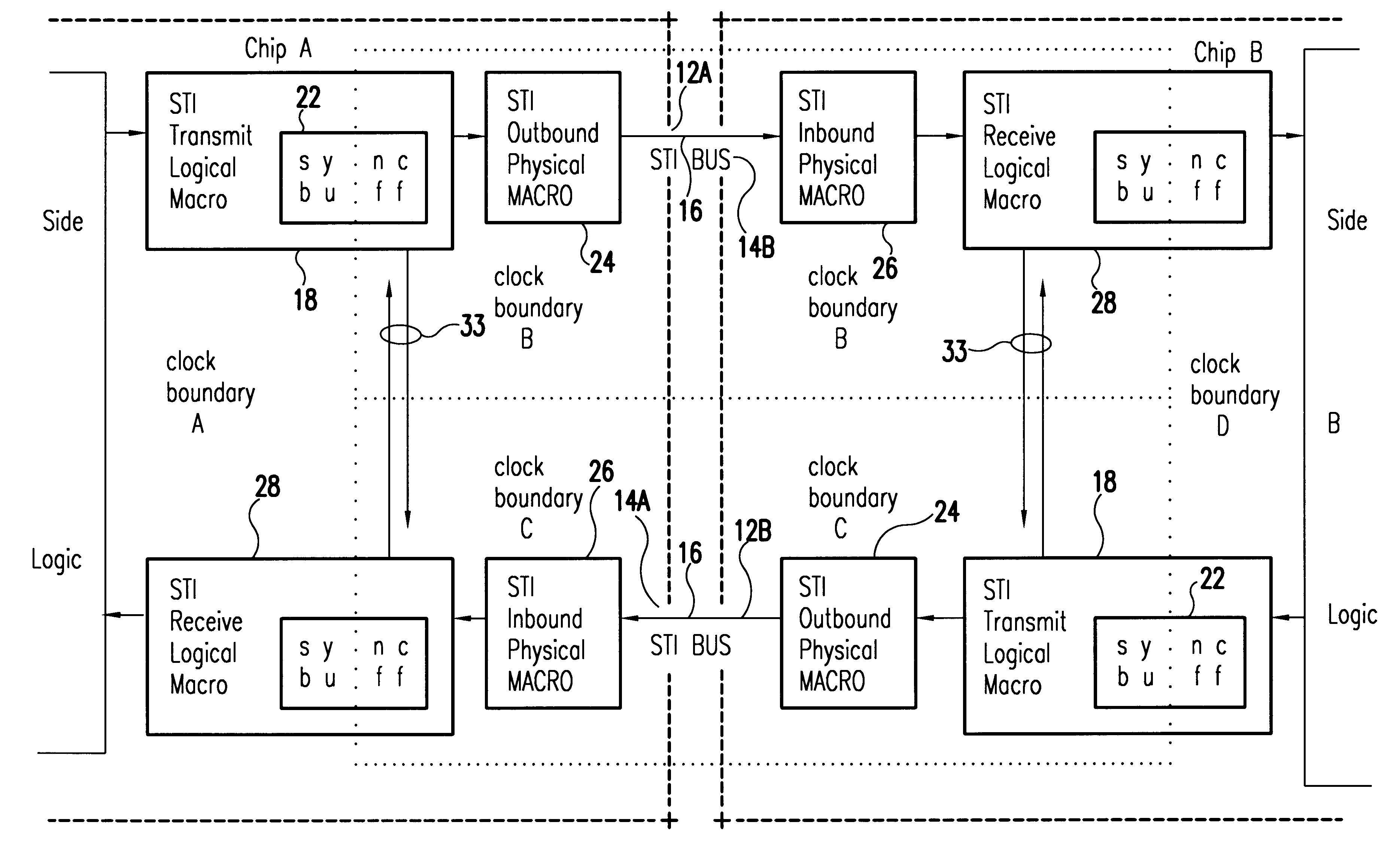
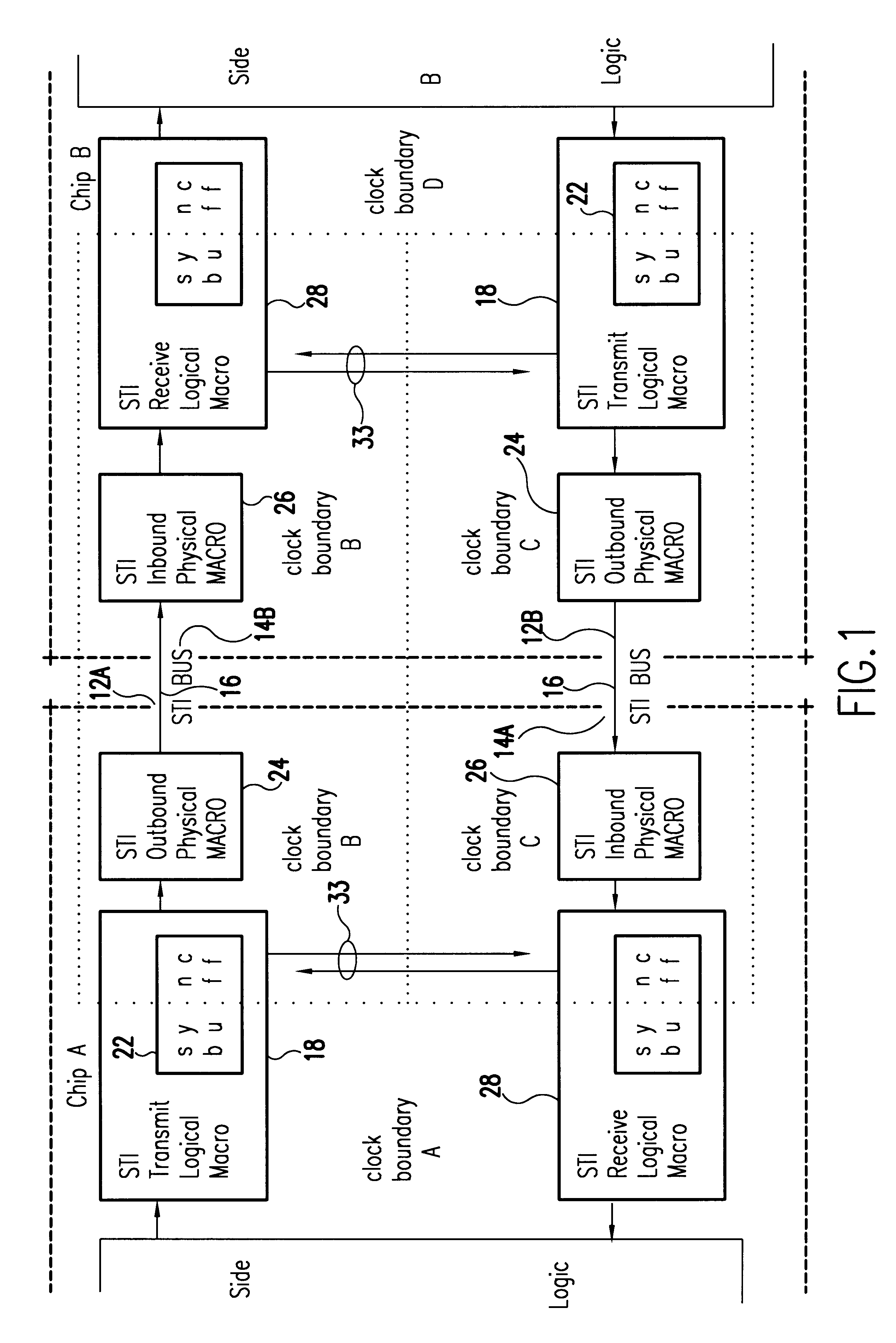
Referring now to FIG. 1 of the drawings, it illustrates one embodiment in which a self-timed interface in accordance with the teachings of this invention can be used. This exemplary embodiment of the self-timed interface provides data communications between two microprocessor chips, labeled here as Chip A and Chip B. However, as will be apparent to those skilled in the art, the self-timed interface of this invention is applicable to provide data transfer between a wide variety of components or nodes.

Chip A has a transmit port labeled 12A and Chip B has a transmit port labeled 12B. Similarly, Chips A and B have receive ports labeled 14A and 14B, respectively. The ports are connected by two self-timed interface busses 16; one for each transmission direction. In this exemplary embodiment of the invention, each bus 16 is one byte wide, and comprised of nine electrical conductors; eight conductors for data and one conductor for a clock signal.

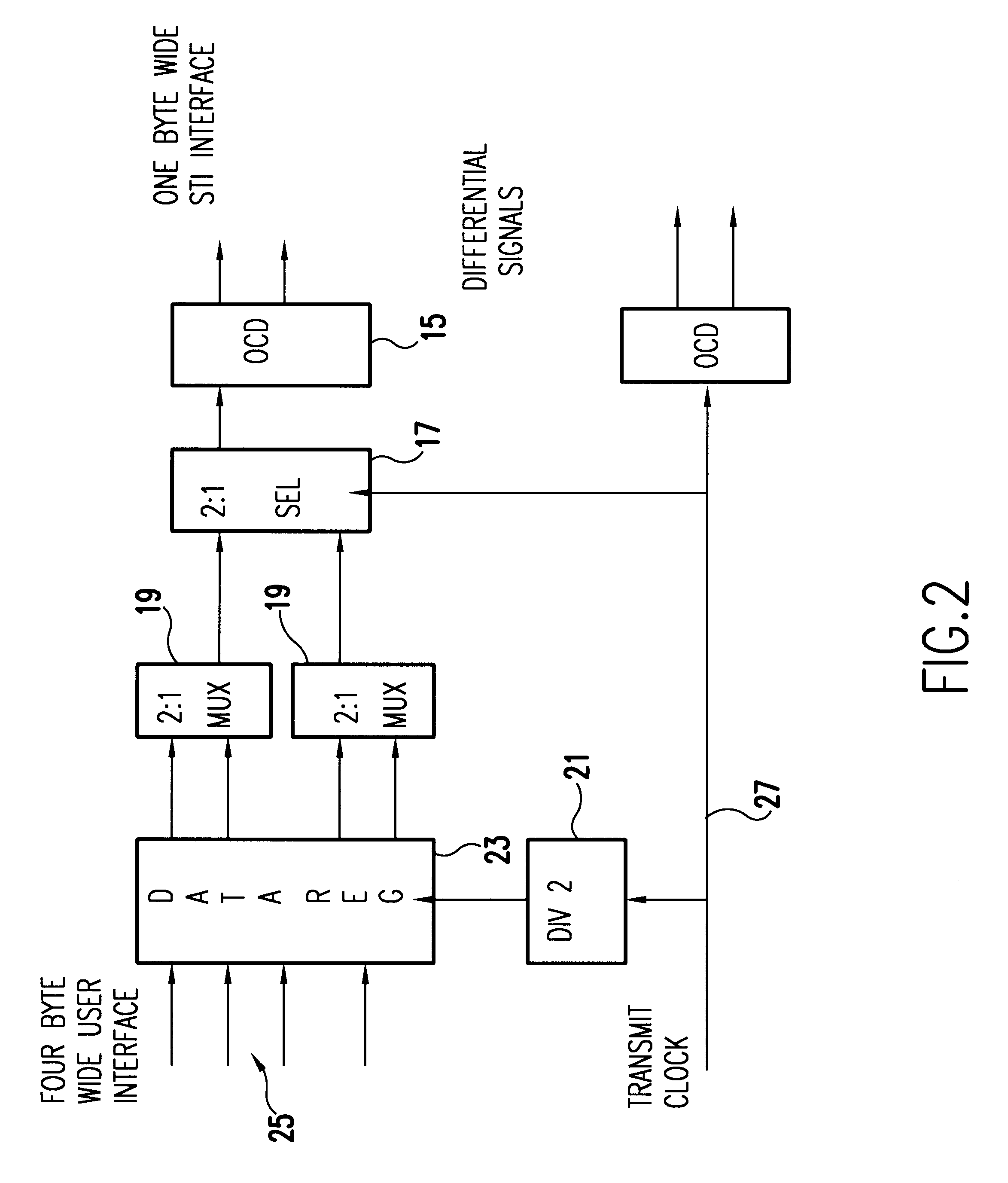
Each transmit port (12A and 12B) includes a t...


PUM


Abstract

A massively parallel system has a self-timed interface (STI) in which a clock signal clocks bit serial data onto a parallel, electrically conductive bus and the clock signal is transmitted on a separate line of the bus. The received data on each line of the bus is individually phase aligned with the clock signal. Digital data is transmitted at high speeds via the parallel bus to provide a scalable communications network for parallel processing systems while eliminating precise bus length and system clock rates as a critical or limiting factor.

Description

The present United States patent application is related to the following United States patent applications incorporated herein by reference:Application Ser. No. 08 / 262,087, filed Jun. 17, 1994, entitled "Digital Phase Locked Loop with Improved Edge Detector," and assigned to the assignee of this application, now U.S. Pat. No. 5,487,095.Application Ser. No. 08 / 261,514, filed Jun. 17, 1994, entitled "Self-Timed Interface," and assigned to the assignee of this application, now U.S. Pat. No. 5,592,553.Application Ser. No. 08 / 261,522, filed Jun. 17, 1994, entitled "Multiple Processor Link," and assigned to the assignee of this application, now U.S. Pat. No. 5,598,442.Application Ser. No. 08 / 261,561, filed Jun. 17, 1994, entitled "Enhanced Input-Output Element," and assigned to the assignee of this application, now U.S. Pat. No. 5,513,377.Application Ser. No. 08 / 261,523, filed Jun. 17, 1994, entitled "Attached Storage Media Link," and assigned to the assignee of this application.Applicati...

Claims


Application Information

Patent Timeline
06 Feb 2001
Publication
US6185693B1
IPC
G06F13/42; G06F13/00; G06F15/17; G06F15/173
CPC
G06F13/4256; G06F15/17; G06F15/17375
Inventors
GARMIRE, DERRICK LEROY; CAPOWSKI, ROBERT STANLEY