Solid-state relay
a solid-state relay and relay technology, applied in the direction of semiconductor devices, semiconductor/solid-state device details, electrical apparatus, etc., can solve the problems of unduly large parallel connected capacitance between the source and the ldmosfet of this structure, and not be satisfactory for minimizing
- Summary
- Abstract
- Description
- Claims
- Application Information
AI Technical Summary
Benefits of technology
Problems solved by technology
Method used
Image
Examples
second embodiment
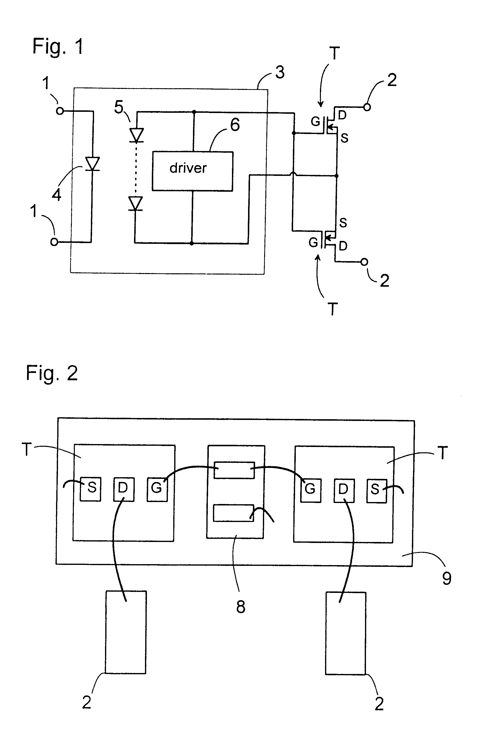
FIG. 6 illustrates a solid-state relay in accordance with the present invention in which each of two MOSFETs T is mounted on a separate supporting plate 9A of electrically conductive material and has its gate connected to a like control unit chip 8A mounted on a separate frame 7. Drain of each FET is electrically connected to each supporting plate 9A formed with an output terminals 2A as an integral part thereof.
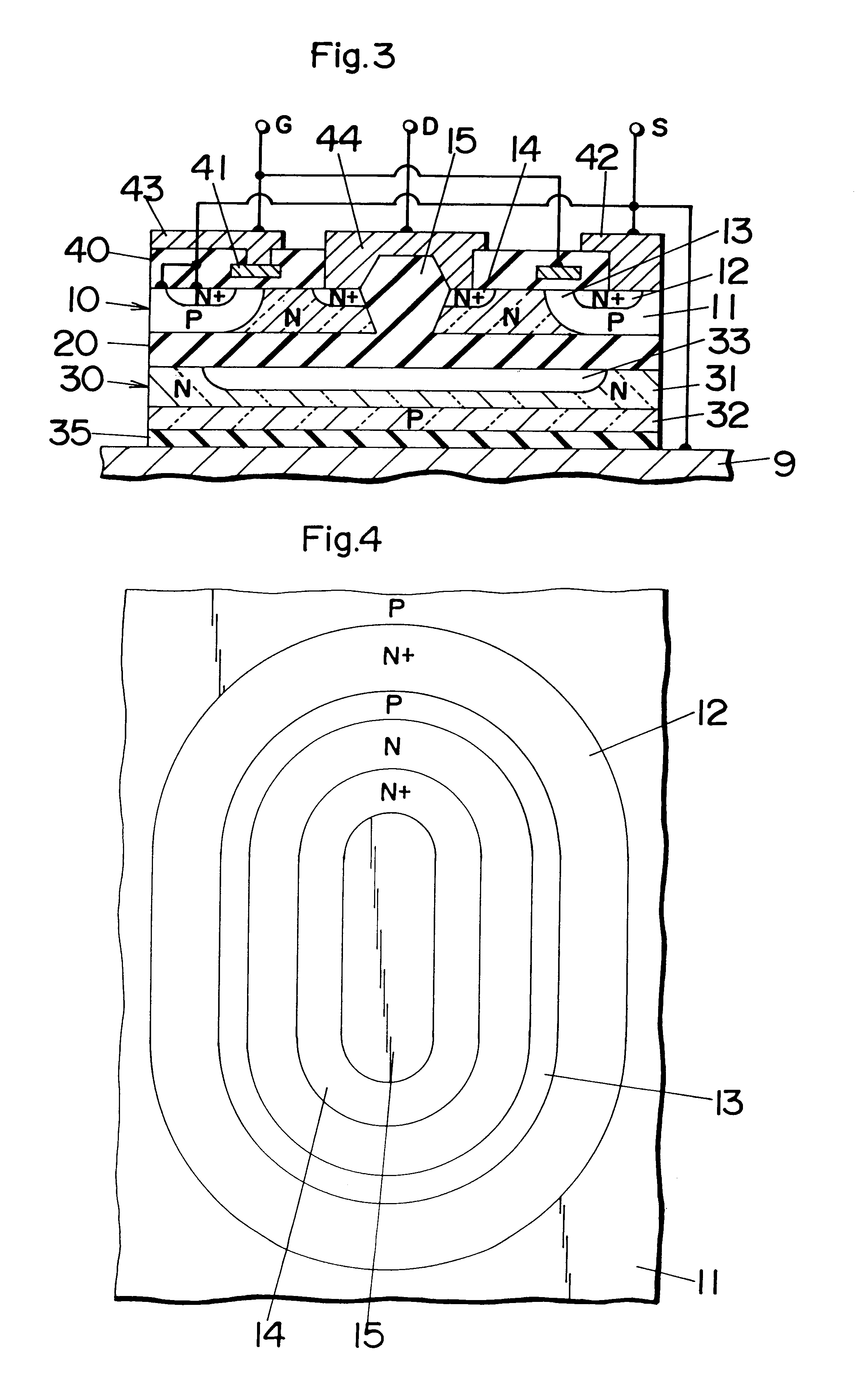
As shown in FIGS. 7 and 8, FET is also of the SOI structure having an N-type silicon layer 10A, a buried oxide layer 20A, and a silicon substrate 30A. A P-type well region 11A of a closed loop configuration is diffused in the silicon layer 10A over the full depth thereof so as to leave therearound a peripheral isolated zone 16. A P-type source region 12A of the like closed loop configuration is diffused in the top surface of the well region 11A to define the source of FET as well as to define a channel 13A between the source region 12A and a confronting inner periphery of th...
first embodiment
Also in this embodiment, the silicon substrate 30A is composed of an N-type upper stratum 31A and a P-type lower stratum 32A placed on the supporting plate 9A through a dielectric layer 35A. The upper stratum 31A includes a cavity 33A of annular configuration in a horizontal plane which is formed at an interface with the buried oxide layer 20A to extend horizontally in an opposed relation to a portion of the silicon layer 10A covering the well region 11A and the separator ring 17. The cavity 33A, the P-N interface between the stratums 31A and 32A, as well as the dielectric layer 35A function to reduce the overall drain-source capacitance in the same manner as explained with reference to the
third embodiment
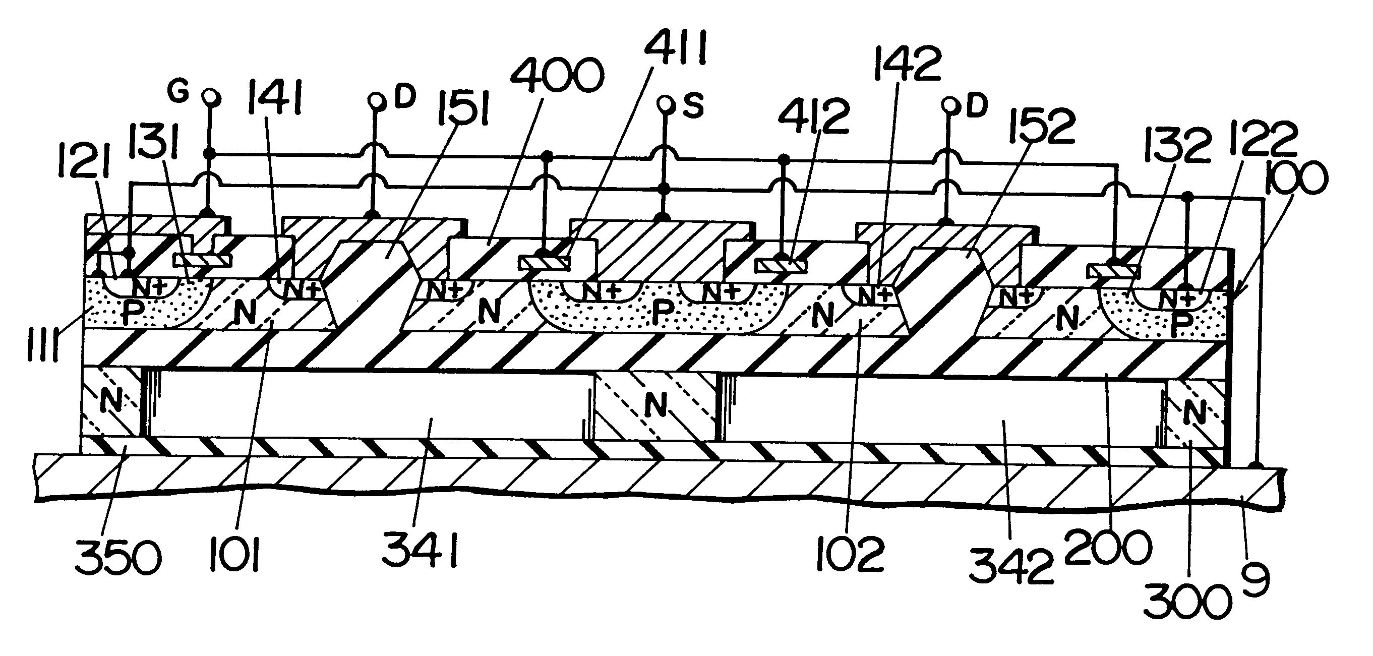
FIGS. 10 to 12 illustrate another structure of SOI-LDMOSFET in accordance with the present invention. FET of illustrated structure is adapted in use for the circuit configuration as shown in FIG. 6, and comprises a N-type silicon layer 10B, buried oxide layer 20B, and a silicon substrate 30B. A P-type well region 11B of a closed loop configuration is diffused in the silicon layer 10B over the full depth thereof so as to leave therearound a peripheral isolated zone 16B. A P-type source region 12B of the like closed loop is diffused in the top surface of the well region 11B to define a channel 13B between the source region 12B and a confronting inner periphery of the well region 11B. An N-type drain region 14B is diffused centrally in the top surface of the silicon layer 10B within a confine of the well region 11B. Locally diffused in the peripheral zone 16B are a pair of P-type land 18 which extend the full depth of the silicon layer 10B and arranged in a horizontal plate to be diame...
PUM
 Abstract
Description
Claims
Application Information


